Posted on
Increasingly, fabricators undertaking whole chip delayering are turning to Broad Ion Beam Etching (IBE), which offers significant advantages over more traditional approaches in delayering today’s larger, denser, and more integrated semiconductors. As implemented in Denton’s Infinity FA, Broad IBE provides the necessary uniformity, minimal damage over large areas, and etch rate normalization across different materials that whole chip delayering demands. There are still ways to optimize the performance of Broad IBE in delayering applications. Here are some tips.
What Broad Ion Beam Etching Is, and What it Isn’t
In Broad IBE, a broad-beam, highly directional source is used to physically remove material from a substrate. Inert argon gas is introduced to the ion beam source, where it is ionized and impelled directionally towards the substrate with high energy. The ions then hit the substrate and the impact removes, or sputters, the material. The effect is something like sandblasting.
This method of etching provides high accuracy and precision through control of the ion beam energy. Because of its low selectivity, it can be tuned to etch uniformly through layers and features comprising multiple different materials. During the IBE process, engineers can also use in situ Secondary Ion Mass Spectroscopy (SIMS) to detect the sputtering of a new layer or material in real time, stopping the etch process at the exact right point.
Because the argon ions are inert, the etching process is entirely physical, making it distinct from approaches such as Reactive Ion Etch (RIE), which uses both chemical reactions and ion etch to remove materials.
RIE is excellent for fabrication and manufacturing, where RIE’s ability to etch straight down with sharp edges enables it to create intricate patterns on substrates with remarkable precision. However, RIE is NOT a good choice for failure analysis, especially for full chip delayering.
Achieving uniform etch rates across the entire substrate surface is a major challenge in RIE. RIE is highly selective, so different materials will etch at much different rates, and the etch will never be planar. Understanding the compatibility between different materials and reactive gases is essential in RIE. The choice of reactive gas greatly affects the selectivity of the etching process.
Other conventional approaches to failure analysis are likewise poorly suited for whole chip delayering. Focused Ion Beam (FIB) etching uses a narrow ion beam to etch and must therefore raster to perform an area etch. The time required makes it impractical to etch an entire IC. “Defocused FIB” is sometimes marketed as a broad ion beam, but its maximum beam is perhaps 2 by 2 mm, far less than the 14 cm of true Broad IBE.
Mechanical polishing, like Broad IBE, is also an entirely physical process. However, because more polishing occurs at the leading edge of any mechanical system, it is prone to “dishing,” where more material is removed at the edges. Mechanical polishing also cannot be reliably stopped at a specific metal layer, requiring constant inspection and repolishing.
Chemical etching, another option, demands expert knowledge on the broad variety of chemicals needed to etch different materials and requires micro polishing steps to clean up the layers for good imaging. Here, Broad IBE delayering is preferred over chemical etching, as it has superior uniformity, less process development than chemical etching, and can be controlled to stop at a specific depth by viewing the etch products in a mass spectrometer.
Top Tips for Using Broad IBE in Whole Chip Delayering
While Broad IBE offers superior performance in etching an entire IC, there are several considerations that can optimize the process:
- The size of the sample, and its placement within the beam
- Preparation of the sample, ensuring that it is perfectly flat
- The material to be etched, to ensure a uniform etch rate
- Controlling the etch depth, stopping at the precise layer of interest
Sample size and preparation of the sample are the most important.
Size of the Sample
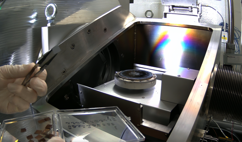
Broad IBE can sequentially etch a whole IC from the top metal layer to the bottom device layer. The technique uniformly delayers the whole chip simultaneously. The beam itself is around 14 centimeters in diameter as it leaves the source, with a uniformity of plus or minus 3% over 100 mm; however, the beam current density is greatest and most uniform in the center of the beam. For a single 10×10 mm IC placed in the center of the chuck, the uniformity is better than plus or minus 0.1%. No other delayering method can approach this.
Sample Preparation
Proper sample preparation is crucial to ensure a clean and representative surface for etching in whole chip delayering. The sample must be depackaged or decapped beforehand, and it has to be absolutely flat. Chemical or mechanical polishing can be used to accomplish this.
Flatness is essential. Broad IBE is largely non-selective, so everything on the chip will be etched at approximately the same rate. If a sample isn’t flat at the beginning, it won’t be flat at the end.
The level of tolerance is the thinness of the layers of interest. If the layers are thinner than the degree of roughness or step heights across the entire chip, it will be impossible to stop at the precise layer of interest without having some interlayer mixing.
Material Considerations
Whole chip delayering demands an etching solution or process that removes material from the component uniformly. The objective is to have the materials etch at the same rate. Because of its low selectivity, Broad IBE excels at this.
RIE, in contrast, is very much a chemical process, where the etch rate can be completely different for different materials depending on the gas chemistry. Etch selectivity of 10:1 or 20:1 is common in RIE, and the ratio can even go higher depending on the materials and the gasses being used.
The etch rate for different materials with Broad IBE is much more even. Even when etching through a refractory metal like tungsten and a very soft material like copper, the difference in etch rates with Broad IBE might only be a factor of two or three.
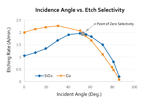
As it turns out, modifying the tilt angle between the target chip and the ion source plays an important role in controlling selectivity and achieving a planar etch across the whole chip. The chart below shows the etch rate of SiO2 and Cu thin films as the incidence angle (tilt) is changed. At around 50 degrees, the etch rates are the same and selectivity drops to zero. Only the angle of incidence was changed in this experiment; all other factors remained the same.
The Infinity FA can also easily accommodate reactive gasses, which can often dramatically accelerate or retard the etch rates of particular materials. For two materials, it may be easy to find a tilt angle that equalizes the etch rates, but in a chip with three or more materials together, it can be complicated to adjust the etch rates. In this case, introducing reactive gasses may offer a solution to better matching the etch rates.
Etch Depth Control and Automated Endpointing
Precise control of the etch depth is essential to expose the relevant features without removing too much material. Mechanical polishing performs poorly at this, as it cannot be reliably stopped at a specific metal layer and requires constant inspection and repolishing. The same holds true with chemical etching and RIE, which will tend to etch all of a given material, regardless of its depth.
There are two reasons why Broad IBE as implemented in the Infinity FA excels at controlling etch depth. The first is the natural repeatability of Broad IBE. The second is the integrated Secondary Ion Mass Spectroscopy (SIMS) module, which can monitor the ions being sputtered from a chip and stop the process when it senses that a particular material is being sputtered.
Because Broad IBE is a physical etch that can be finely tuned, just paying attention to time and level of power will result in the same, consistent results within a few percent. The configuration of the source keeps the plasma fully remote from the substrate, meaning that it is unaffected by anything going on in the etching. The result is that even etching on time alone, the repeatability will be better than 1%.
This natural repeatability and nanometer-level control is complemented by the SIMS module, which can identify when a layer of interest has been reached and allows precise endpointing. The SIMS automated spectroscopy monitors the composition of the material removed, stopping etching once a pre-set signal has been reached. This makes it possible to create highly repeatable recipes that can be easily automated. The engineers in Denton’s application lab can help develop the optimal recipe.
Conclusion
It’s critical to use the right tool for a task. While there are a wide variety of different approaches to etching ICs for failure analysis – such as RIE, FIB, mechanical polishing and chemical etching – Broad Ion Beam Etching (Broad IBE) is best suited for delayering an entire semiconductor. The other approaches use a beam that is too focused, and therefore poorly suited for etching the large areas involved, or rely on mechanical or chemical means that result in damage or other artifacts.
As implemented in Denton’s Infinity FA, Broad IBE provides the necessary uniformity, minimal damage over large areas, and etch rate normalization across different materials whole chip delayering demands.
If you’d like to learn more about how Broad IBE and the Infinity FA might suit your needs, read this article in EDFA Digital, “Whole-Chip Delayering for Failure Analysis and Quality Assurance,” or watch this previously recorded, hands-on demonstration of Denton’s Broad IBE in action.