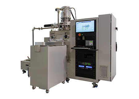
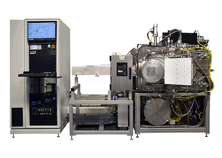
See how Denton Vacuum has pioneered thin film for 6 decades.

Advanced Semiconductor Applications

As semiconductor device architectures continue to shrink and conventional deposition technologies reach their fundamental limits, ion beam deposition and ion beam etch are under investigation for manufacturing next generation chip technology.


Low Resistivity Contacts

While magnetron sputtering tools have traditionally been used for metal interconnects, IBD tools can produce thin, dense, and contamination free films which offer significant advantages.


Ultrathin Barriers

While CVD tools have traditionally been used for dielectric barriers, IBD tools can produce thinner and denser pinhole-free films which offer significant advantage.


Low Damage Etch

Plasma etch damage to the metal under-layer is minimized by using a low energy etch for the last few nanometers being etched away, leaving a thinner dead layer caused by higher energy etch techniques.


Featured Solutions For Advanced Semiconductors