What is Thin Film Deposition?
Thin film deposition is the process of creating and depositing thin film coatings onto a substrate material. These coatings can be made of many different materials, from metals to oxides to compounds. Thin film coatings also have many different characteristics which are leveraged to alter or improve some element of the substrate performance. For example, some are transparent; some are very durable and scratch-resistant; and some increase or decrease the conductivity of electricity or transmission of signals.
Thin film deposition is an important manufacturing step in the production of many opto-electronic, solid state and medical devices and products, including consumer electronics, semiconductor lasers, fiber lasers, LED displays, optical filters, compound semiconductors, precision optics, microscopy & microanalysis sample slides, and medical implants. There are a few different technologies and methods that can be used to apply thin film coatings, and an array of tools and equipment that can be used to streamline or enhance the thin film deposition process.
There is no one-size-fits-all, perfect thin film deposition system or method. Your technique and configuration of choice depends on the performance and production requirements that are unique to your application.
What is Physical Vapor Deposition (PVD)?
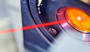
Physical vapor deposition (PVD) describes a group of thin film deposition techniques that involve vaporizing a solid material in a vacuum, then depositing that material onto a substrate. Coatings created in this manner are highly durable, and resistant to scratching and corrosion. PVD is useful in the production of devices ranging from solar cells to eyeglasses to semiconductors.
The benefits of PVD are numerous, and include the creation of a hard coating that is resistant to corrosion and scratching. PVD also creates thin films that can tolerate high temperatures. Denton’s PVD systems can be integrated with in-situ controls that allow for feedback and stability throughout the process.
Potential drawbacks of PVD include cost, as these methods may require a larger investment than other thin film deposition processes. The cost can also vary among PVD methods themselves. For example, evaporation is a lower-cost type of PVD, while ion beam sputtering is a rather costly option. Magnetron sputtering is more expensive than other methods, but has better scalability.
A variety of techniques fall under the PVD umbrella. For a comparison of these method types, read: Which PVD Method to Use: Magnetron Sputtering v. Evaporation.

Evaporation
There are multiple types of evaporative deposition:
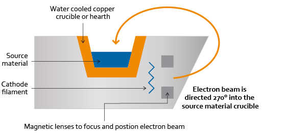
- E-beam evaporation (electron beam): In this process, a highly-charged electron beam evaporates the target material. The evaporated material is then deposited onto the substrate, and the atoms formed create the thin film. This process is often used for optical thin films such as solar panels, glasses and architectural glass.
- Ion assisted deposition (IAD): This process produces films with less scatter than typical evaporation. For a deeper dive into IAD, download our infographic.
- Thermal evaporation: In this simpler form of PVD, a resistive heat source heats the target material until vapor pressure is produced. The evaporated material then coats the substrate, forming the thin film. It is used to deposit metals such as silver and aluminum for OLEDS, solar cells and thin film transistors.
Magnetron Sputtering
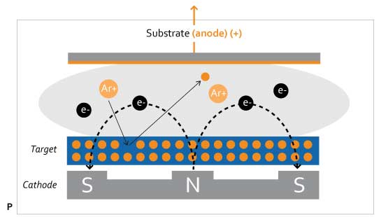
Magnetron sputtering is a versatile, plasma-based coating technique. In this process, magnetically confined plasma is created near the surface of the target material. Ions from that plasma collide with the target material, and the atoms ejected from those collisions are what are “sputtered”, or deposited onto the substrate to create the thin film. It is often used for metallic or insulating coatings for optical and electrical purposes.
Ion Beam Sputtering
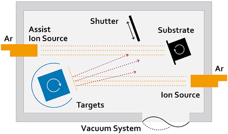
Ion beam sputtering (IBS) is also called ion beam deposition (IBD). This process uses an ion source to sputter the target material—either metallic or dielectric—onto the substrate, forming the thin film. Thin films created through ion beam sputtering are of a high quality, and have very precise thickness due to the monoenergetic ion beam used. This process is often used to create coatings for precision optics and semiconductors, where the utmost precision is required.
Pulsed Laser Deposition (PLD)
Pulsed laser deposition is a type of evaporation process that uses laser pulses to evaporate the target material. This produces a plume of plasma that then deposits onto the substrate, forming the thin film. While optimizing this process can require more time and effort than other methods, due to the many variables at play, its benefits include high deposition rates and a streamlined process, as well as no filaments for easier maintenance.
What is Chemical Vapor Deposition (CVD)?
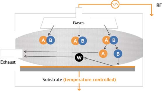
Chemical vapor deposition (CVD) describes a group of thin film deposition techniques in which a substrate is placed into a vacuum chamber, two chemical precursors are heated, which causes them to vaporize. When they meet on the substrate surface, a chemical reaction occurs to form a high-performance thin film coating. CVD is useful in creating coatings for a wide variety of applications including medical devices, automotive components and silicon wafers.
Benefits of CVD methods include the ability to use these processes on a wide variety of substrates, as well as the ability to coat intricate or complex topographies. Thin films created through CVD also typically maintain their bonds well in high-stress environments.
Some drawbacks may include limitations in size, which is dependent on the size of the vacuum chamber, as well as that most methods typically require a higher temperature to drive the chemical reactions. It can also be difficult to mask the surface of the coating.
There are a variety of CVD methods:
Atmospheric Pressure CVD
In this process, which takes place at normal, or atmospheric, pressure and a lower temperature than other methods, the substrate is exposed to at least one volatile precursor. The precursor(s) react on the surface of the substrate to deposit the thin film. It can be used to deposit doped and undoped oxides, and the deposition is fairly quick. Thin films produced by this method are low-density and have moderate coverage.
Low-Pressure CVD
In low-pressure CVD, heat is used to break down a precursor gas inside the chamber where the reaction will take place. This causes the reactive gas to react with the substrate when it is injected into the chamber, and this reaction creates the thin film coating. Low-pressure CVD is commonly used for the deposition of materials including polysilicon and silicon nitride, and can be useful for batch processes. Coatings created with this process are more uniform and feature fewer defects, but the process requires a higher temperature which can limit the materials available to use.
Ultrahigh Vacuum CVD
In ultrahigh vacuum CVD, the substrate is exposed to precursor gases in an ultrahigh vacuum (<10^{-6} Pa). These precursors then react and deposit onto the substrate, forming the thin film.
Atomic Layer Deposition
While atomic layer deposition falls under the CVD umbrella, it differs in that precursor materials are kept separate during the reaction. In this process, the reaction occurs due to sequential pulsing of precursor vapors—one atomic layer is formed during each pulse. Pulses are repeated until the thin film reaches its desired thickness. Benefits of atomic layer deposition include high quality defect-free coating, as well as improved thickness uniformity.
Plasma-Enhanced PIB-CVD
Plasma-enhanced CVD is a lower-temperature alternative to standard CVD, and is often used in the production of electronic devices. One common application for PIB-CVD coatings is to protect these devices from corrosion. It can create, for example, high-quality silicon dioxide (SiO2) film at 300°C to 350°C as opposed to the temperature range of 650°C to 850°C required by standard CVD to create similar films. In plasma-enhanced PIB-CVD, a pair of reactive gases are excited to create a plasma. This causes a chemical reaction that results in the thin film being deposited onto the substrate.

Thin Film Markets & Applicable Coatings
Thin film coatings are used in a wide range of applications for many purposes. They can be used to protect displays from scratches or environmental exposure, create a specific degree of reflectivity on a lens or build layers of metallization on semiconductor wafers. Some of the biggest markets that are served by thin film coatings are opto-electronics and display, semiconductors, medicine and healthcare, and microscopy.
Opto-electronics and Display
Precise, uniform thin films are absolutely critical to many applications in opto-electronics.
Common applications include:
- Fiber optic lasers for telecom and wireless comm systems
- Fiber lasers for metal cutting
- Consumer electronics
- Laser diodes for 3D sensing
- LED/OLED displays
Common coatings used across this industry are:
- AR/HR coatings
- Optical filters
- TCO coatings
- Indium bump coatings
- DLC coatings
AR/HR Coatings
Anti-reflectivity/high reflectivity coatings are both used to change an optic’s degree of reflectivity, but in opposite ways. An AR coating increases the transmission of light waves to reduce surface reflections. An HR coating increases surface reflectance to create mirrors that reflect all light of a given wavelength.
AR coatings are commonly used in eyeglasses, photographic lenses and solar cells, and any application in which reflection would diminish performance or user experience. Laser applications use both AR and HR coatings.
Common deposition methods:
- Ion assisted deposition
- Magnetron sputtering
- Ion beam deposition
Indium Bump
Indium bump deposition is used primarily in focal plane arrays for IR imaging. As feature sizes get smaller, manufacturers need a more effective solution than indium bump electroplating. Indium bump deposition offers high shear strength, good lift-off and collimation control for such purposes.
Maximum yield indium bump deposition is achieved with a cooled substrate stage for temperature control, and collimation control that enables direct deposition. When both temperature and geometry are optimized, so is the crystal structure, enabling high shear strength and improving performance.
Common deposition methods:
- E-beam evaporation
- Thermal evaporation
Transparent Conductive Oxide Coatings (TCO)
These are transparent, electrically conductive film coatings that are commonly used in electronics. They are particularly common in displays. They offer improved precision and higher yield, and typically have a high transmittance and low resistivity. Specific applications for TCO coatings include photovoltaics, liquid crystal displays, OLEDs and touchscreens.
Common deposition methods:
- Magnetron sputtering
Optical Filters
Optical filters are similar to AR/HR coatings in that they are used to modify light waves within an optical system. The difference here is that it’s for the purpose of filtering light through the optic, not just to change reflectance on the surface.
Very precise coatings are required to accurately control reflectance, transmittance, absorbance and resistance. Filters are commonly used in photolithography, image enhancement, image splitting, color match imaging and Raman spectroscopy.
Common deposition methods:
- Ion assisted deposition
- E-beam evaporation
- Magnetron sputtering
Diamond-like Carbon Coatings (DLC)
DLC coatings are integral to consumer electronics, particularly the display market, where they are used to protect displays and LEDs. These coatings offer improved hardness, chemical and scratch resistance, high thermal conductivity and electrical resistivity.
With DLC coatings, product life in the end-use application is extended; commonly used on displays, sensors and flexible semiconductors. Displays also require other protection for durability and to extend product lifetime. For example, hydrophobic coatings are needed to make touchscreens water resistant and resistant to wear from constant contact with skin oil.
Common deposition methods:
- PE-CVD
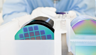
Semiconductors
Semiconductors require their own specific types of thin film coatings in order to conduct electricity and enable data transmission/storage. There are a number of coating options available for semiconductor applications, including contact coating, gold coating, under bump metallization, DLC coating, barrier overcoats, piezoelectric alloys and precision alloys.
Common applications include:
- LEDs
- Photodetectors
- IR detectors
- Focal plane arrays
- RF power transistors
Many of these applications require a notably high volume for manufacturing, and these applications need a thin film deposition system that supports that volume and throughput.
Metallization
One of the most common methods for coating semiconductors, metallization involves depositing a metal film over a dielectric film (or layers of both) onto a semiconductor wafer. Adhesion layers and conduction layers are deposited to create gate stacks, allowing the device to supply an electric current or provide an electronic signal. Metallization requires good adhesion between the thin film coating and the wafer, otherwise performance will be adversely affected.
Common deposition methods:
- Magnetron sputtering
- E-beam evaporation
Medical Applications
Medical implants and similar devices often require coatings for protection. Coating specs need to be very precise and particular to meet medical regulations and standards, such as those specified by the FDA. Safety and health is of the utmost importance in this market so consistent performance needs to be ensured for every device and coating. Implants will face exposure to human tissue and other biological substances/materials, so they need to be protected from degradation without harming the person.
Common coating solutions for the medical market include DLC and biocompatible hard coatings.
Biocompatible Hard Coatings
Biocompatible hard coatings are often made up of titanium nitride, titanium aluminum nitride, chrome nitride or titanium carbo-nitride. They are used to increase the durability/lifetime of biomedical implants, and help with dimensional stability for stimulation electrodes, such as those used in implantable neural prostheses leads.
Common deposition methods:
- Magnetron sputtering for conformal coatings for wear resistance/color coding
- PE-CVD on TiN coatings to enhance durability
Thin Film Characteristics/Performance
There are a number of different properties that can affect thin film performance. The properties that manufacturers need to focus on vary depending on specific application needs. Precision optical coatings often require a very tight precision and repeatability, for instance, whereas good adhesion is an important requirement for high-volume metallization coatings.
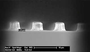
Film Thickness
This refers to the thickness of the thin film coating. Your thin film coating needs to fall within the right thickness parameters for your specific application in order to ensure performance.
Some applications require a very fine, precise coating, for example, to allow for the right degree of light transmission. Other applications require a thin film coating for durability and protection, so they can be a little bit thicker and may not need to be so precise.
Thickness also has big implications for next-gen products. Flexible displays are starting to mature on the market for consumers but they require thinner film coatings so that they can bend as needed.
Film Uniformity
Uniformity is one of the most important properties across all applications and coatings. If thickness distribution is not even, it could inhibit durability and performance for the entire film. Some substrates also have a more complex topography, with bumps and vias present, but the thickness also needs to remain consistent across the surface.
Uniformity affects other important production factors such as yield and cost of ownership, along with thin film performance. Better thickness uniformity means more usable parts are produced, but the costs of achieving uniformity with a particular system or configuration must also be considered and weighed.
Reflectivity
The degree of reflectance is particularly important for AR/HR coatings used in laser applications. A thin film’s reflectivity determines if it will act as a mirror and reflect light back out, or allow light to pass through as in an optical filter or laser diode.
Whether it’s reducing the glare on a pair of glasses or a VR headset, or filtering out visible light in a smartphone’s face recognition software, reflectivity is a very important property to control for in many applications in the opto-electronics and optics spaces.
Grain Size
Solid metals are composed of individual crystallites or particles, and the size of these particles is referred to as grain size. Grain size itself determines many other properties specific to the metal, most notably its density. High energy and higher migration between particles leads to a smaller grain size, while lower energy and lower migration leads to a larger grain size.
Density is inversely proportional to the grain size, so for applications requiring a high density, you want a coating that has more migration between particles and a smaller grain size. By controlling the grain size and density, you can also improve the thin film’s wear resistance and strength.
Yield
Yield is determined by the number of usable parts that are produced by your thin film deposition system. It’s largely determined by your configuration’s precision and repeatability. Reaching a high yield is also impacted by performance requirements. If your coating requires very tight specs, you’ll need to prioritize precision to hit within those specs in order to raise your yield.
It’s important to consider exactly what an application requires in order to determine what an acceptable yield is. For example, your application may only require a spec to fall within +/- 5% of a certain setpoint. If you improve precision beyond that, it’s not going to significantly raise your yield, so it may not be worth the investment.
Throughput
Throughput refers to how many substrates your thin film deposition system can coat per hour. It’s one of the most basic measures of system efficiency and ties into your ROI and cost of ownership significantly.
For high-volume applications, having a system that can keep up with high throughput requirements is critical. Lower volume applications may not require such a high throughput, allowing you to focus on performance-related properties instead. For any production volume, it’s important to prioritize throughput needs with thin film performance demands in order to maximize COO.
Adhesion
Adhesion determines a thin film’s stability. If a coating has good adhesion, it will stick tightly to the wafer or substrate, which raises production yield and also increases overall reliability. Good adhesion leads to a better user experience thanks to improved device performance and a longer lifetime.
Moisture and hydrocarbons can both be detrimental to adhesion, so a pre-cleaning process may be needed to remove those molecules. To improve adhesion in metallization, you also need to prevent oxidation between the adhesion and conduction layers. This can be done by coating multiple layers without breaking vacuum.
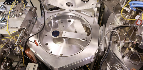
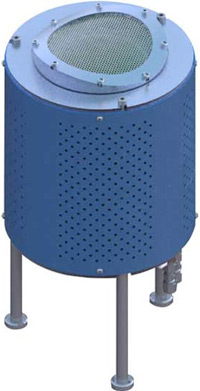
Thin Film Deposition System Tools
There are a number of different tools that can be integrated with a full thin film deposition system, and they each have their own benefits. They can help achieve desired film specs, monitor the deposition process or increase automation and efficiency. While adding these tools may require a bigger investment up front, the process enhancements and control may be well worth it depending on your specific application needs.
Front-End Options
Front-end options are really common additions for manufacturers who are trying to introduce automation to the deposition process. These tools help automatically load the deposition module with varying degrees of efficiency, and they are worth the investment when higher throughput needs are required.
Having a thin film deposition module or configuration that is compatible with all front-end options is really important for scalability. If your system is scalable you will save on capex costs and gain a higher ROI on what you do spend on the equipment.
Types of front-end options:
- Single wafer load lock: This type of load lock can load a deposition chamber with one wafer at a time.
- Cassette load lock: An upgrade in terms of efficiency, a cassette load lock will load the system with up to 25 wafers at once.
- Cluster tool: This is the most efficient type of front-end option when it comes to throughput. A cluster platform can combine multiple deposition modules with cassette load locks, and features a robotic arm that moves the wafers from the load locks through the different chambers for coating.
Ion Sources
Ion sources are used to create specific ion species with the purpose of controlling thin film qualities during deposition. By adding an ion source to your configuration, you can enhance density, optical transmission, thickness uniformity, smooth interfaces, adhesion and vertical sidewalls.
All ion sources are equipped with a neutralizing method, to prevent the substrate from becoming too charged by the ion beam. Some ion sources include a hollow cathode or a filament to produce electrons and neutralize the charge. Other ion sources are self-neutralizing, meaning they can neutralize without a filament or cathode.
Self-neutralizing ion sources are better for reducing maintenance frequency and costs, but often require a bigger upfront investment. If precision is a requirement for your application, a self-neutralizing source may be the way to go. Otherwise a filament or hollow cathode should be suitable and won’t drive up cost of ownership.
In-Situ Controls
In-situ controls provide feedback on the deposition process and thin film formation by observing it in real time. Controls allow you to make adjustments during the deposition process so you can ensure the coating is hitting the necessary specs. Thanks to these critical adjustments, you gain better process control and more precise thin film coatings.
There are several different types of in-situ controls:
Plasma Emissions Monitor
A PEM is often used to improve throughput and yield while ensuring that performance-related properties do not fall outside of the desired setpoints. PEM involves monitoring reactive gas flow during the deposition of oxide and nitride films. It prevents target poisoning by maintaining the gas intensity at a constant setpoint. A PEM is a good option for applications like high-rate optical film deposition, process quality control, metallurgical research and process control, and process R&D.
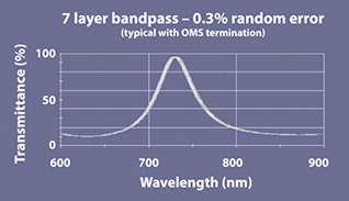
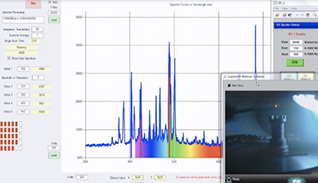
Optical Monitoring System
An OMS is ideal for precision optics applications where feedback is needed as an optical film is produced. Similar to a PEM, an OMS offers excellent repeatability and yield. The system monitors an optic’s properties by observing its reflection or transmission through a substrate or witness chip. Based on the reflection, the OMS will signal the end of the deposition when the desired optical thickness has been reached. It’s a desirable control for applications like AR/HR coatings, laser facets, optical sensors and filters, band pass filters, IR filters and coatings, neutral density filters, metallization and beam splitters.
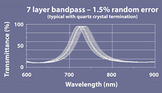
Quartz Crystal Monitoring
QCM differs from an OMS because it is used to measure the physical thickness of a film, not the optical thickness. QCM involves indirect monitoring of a separate chip, not the actual substrate, so it requires calibration within the tool. The QCM provides a linear change in crystal frequency to signal the film thickness on the crystal. It’s a cost-effective control that is best applied when there are broad specifications on optical properties of metal and optical films.
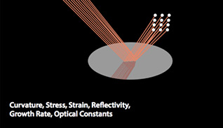
Ellipsometer/Reflectometer
Ellipsometers and reflectometers can be used during the thin film deposition process to provide feedback for Statistical Process Control. These in-situ controls are good options for monitoring curvature, stress or reflectivity.
Process Software
Software is an integral part of any thin film deposition system. Reliable software allows you to execute critical process steps with accuracy and efficiency. If you’re using a front-end option or scaling your system up for high-volume manufacturing, having a software package that enables automation is integral.
Your software should be able to handle your specific throughput and production requirements while also delivering precision and performance. Important features in a software package, particularly for high-volume or demanding applications, include a recipe builder, automated scheduler and on-tool, customizable charting capabilities.