Automation: Sputtering vs Evaporation, Which is the Better Choice?
Posted on
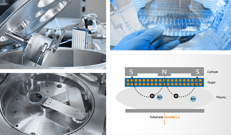
Manufacturers are increasingly seeking to automate as much of the thin film deposition process as possible, working towards a complete “lights out” operation. As a result, manufacturers are moving away from evaporative physical vapor deposition (PVD) methods to using magnetron sputtering. Here’s why. While both evaporation (by thermal resistance or e-beam) and sputtering (either magnetron… Read More