Desk V
The Desk V Sample Preparation system, equipped for both evaporation and sputtering, is a high productivity solution that delivers exceptional, consistent and highly repeatable results.
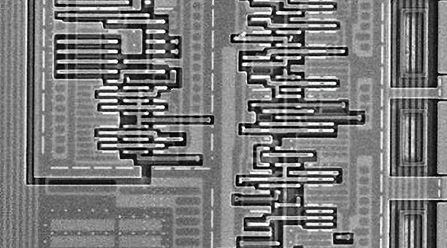
View DetailsElectron microscopy techniques enable researchers and engineers to obtain high resolution images at magnifications up to 500,000X that of the naked eye. When imparting a sample with a high-energy beam of electrons, those electrons interact with the surface and emit secondary electrons as well as back-scattered electrons. These particles are detected and used to generate an image of the sample with amazing detail and high resolution.
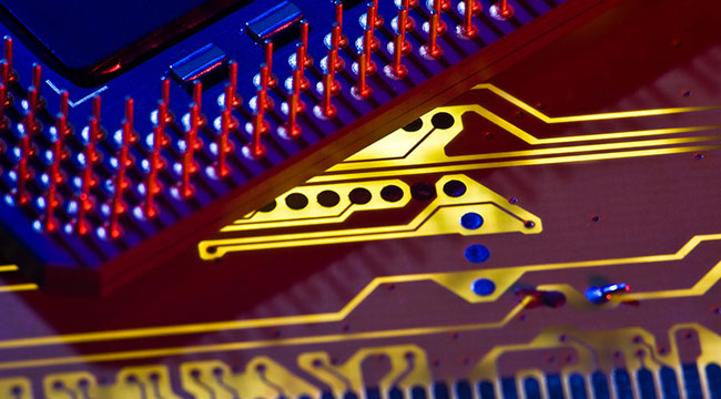
Imparting certain specimens with a beam of electrons is not trivial. In the case of SEM imaging techniques, if the sample is not electrically conductive, the excess electrons will not find a path to ground and the result is what is commonly referred to as “sample charging.” The excess electron energy from the beam is stored on the sample surface and the collected signals will not generate the image as intended. Also, in cases where the sample is temperature sensitive, the electron beam can damage or even melt the non-conductive sample. Coating such samples with a continuous, conductive thin film offers the excess electrons a path to ground so they can dissipate. For TEM, coating grids with carbon can help with samples that are extremely fragile or not embedded in a matrix for support. The carbon is also conductive, which provides a path for the electrons, just as the metal coatings do in SEM applications.
Microscopy is not only important to researchers who are trying to understand more about the structure, properties and performance of materials. It is also critical for processing forensic evidence, consumer product quality assurance, and health and safety testing. Researchers, scientists and engineers in these fields require the utmost consistency and reliability in their results, and often, microscopic samples will require thin film coatings to adequately prepare them for imaging. Denton Vacuum has developed repeatable and dependable solutions using thin film deposition for the preparation of samples for study with electron microscopes. For more information about TEM or SEM sample prep solutions, read the page below, or if you’re looking for a specific part, start browsing our online inventory.
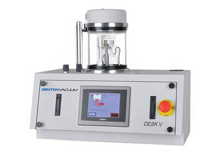
The Desk V Sample Preparation system, equipped for both evaporation and sputtering, is a high productivity solution that delivers exceptional, consistent and highly repeatable results.
View Details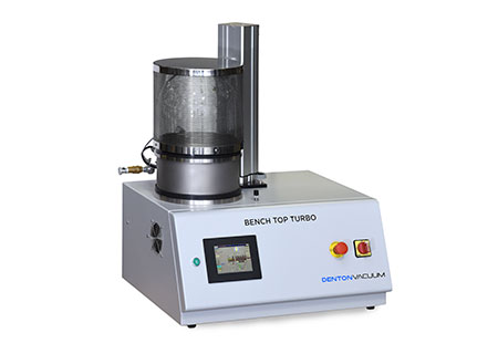
The flexible and compact Benchtop Turbo for thermal evaporation and sample preparation is a powerful, versatile high vacuum evaporation and sputtering system.
View Details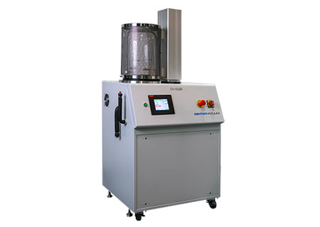
The DV-502 evaporates many of the metals involved in optical coatings, metalizing and electron microscope specimen preparation, including carbon, gold, gold/palladium and platinum.
View Details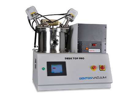
The Desktop Pro is a compact flexible, versatile sputtering system designed for materials research and development.
View Details