Posted on
Denton Vacuum is currently conducting cutting-edge research on how its proprietary ion deposition processes could be used in the manufacturing of quantum computing devices. Denton’s research has the potential to transform the scalability and cost-effectiveness of quantum device production.
The Challenge in Building Quantum Devices
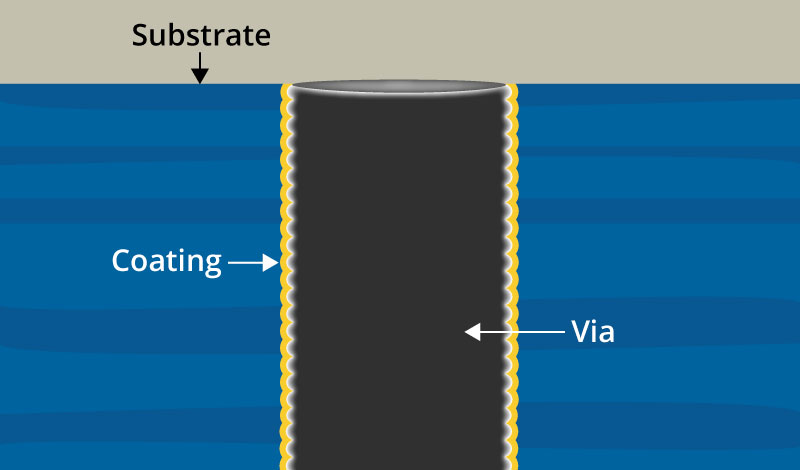
Building quantum devices demands specialized processes that can deposit ultrapure, dense, defect-free crystalline thin films on complex 3D structures such as Through-Silicon Vias (TSVs) and Through-Glass Vias (TGVs) in vertically integrated packaging.
For hardware manufacturers, the challenge in 3D packaging is no longer just about designing the architecture; it is about the physical reality of manufacturing it. Specifically, the difficulty lies in achieving conformal coating on the microscopic structures that enable 3D packaging. The standard process used to create TSVs and TGVs results in “scalloping” along the vertical surfaces of the vias, which are difficult to coat.
There are two different potential applications being tested in Denton’s research. The first is the deposition of a copper seed layer for TGVs used in advanced packaging. The other is deposition of a superconducting film on the sidewalls of TSVs. Both applications require high aspect ratios on these nearly vertical and difficult-to-reach structures.
Orders of Magnitude Faster than ALD
Currently, atomic layer deposition (ALD) is the only method capable of depositing the conformal coatings required in building quantum devices. Unmatched in its control over layer thickness and stoichiometry, ALD deposits conformal coatings on 3D structures with tight atomic-level thickness control.
Unfortunately, ALD is extremely slow. ALD effectively builds films molecule by molecule, making it an expensive process that cannot be easily scaled to production-level volumes.
Denton’s Plasma Ion Beam Assisted Chemical Vapor Deposition (PIB-CVD) method can, theoretically, come close to matching the stoichiometry and conformality offered by ALD while beating ALD’s deposition rate by four to six orders of magnitude. ALD deposits in the range of tens of nanometers per hour. By contrast, Denton’s PIB-CVD method deposits a micron a minute! Microns are millionths of a meter. Nanometers are billionths of a meter, one thousand times smaller than a micron.
Denton’s early research is producing highly conformal films.
PIB-CVD can be easily integrated into Denton’s Discovery and Phoenix platforms.
The key determinant in Denton’s research is the aspect ratio of the films being deposited on scalloped vertical surfaces, such as those in a TSV or TGV. The higher the ratio, the more straight-line vertical the lining of the Via. The goal is a conformal coating that is the same thickness everywhere, regardless of 3D shape, which is highly related to sidewall coverage.
There are a range of proprietary technologies that Denton can bring to bear on building tight aspect ratios:
- Dual Collimation. With Denton’s dual collimation method, incorporating both long-throw and physical collimation, Denton should be able to achieve a 3:1 aspect ratio.
- HiPIMS. With high-power impulse magnetron sputtering (HiPIMS), Denton is likely to achieve a 5:1 aspect ratio.
- PIB-CVD. The ultimate goal is a 10:1 aspect ratio, as that is what is needed for the most demanding quantum applications. Denton’s PIB-CVD should be able to achieve this aspect ratio, and Denton’s research is intended to confirm this.
The industry could end up with a range of different options to create conformal quantum-capable coatings at scale at a variety of different price points. Not every quantum application requires a 10:1 aspect ratio, but production scalability is a challenge at all levels of capability. There are also many other applications where such high aspect ratios are needed.
Setting the Stage for Transformation
It is difficult to understate how transformative this could be for the emerging industry surrounding quantum devices, which is currently hampered by seemingly insurmountable problems with scalability.
Talk to us today if you would like to learn more about the cutting-edge research Denton is conducting on thin films for quantum devices.