
Posted on
The explosion of Artificial Intelligence (AI) and the building of the high-powered data centers that support it has highlighted the potential end of Moore’s Law, a shift that represents an opportunity and a challenge for thin film deposition technologies.
The Hidden Problems Behind the Growth of AI
To put it plainly, the growth in AI workloads is scaling faster than the 2x improvement in compute power every 18 months postulated by Moore’s Law. Training compute loads are growing about 750x every two years, while the size and complexity of Large Language Model (LLM) AIs are growing 410x.
Despite their potentially enormous compute capabilities, the general processing units (GPUs) used in AI applications are limited by their ability to move volumes of data quickly between the processors and memory. Interconnections remain a bottleneck, resulting in a brute force approach to scaling where ever-larger numbers of processors are being used.
As a result, AI data centers are driving massive demands for electricity and water. GPU-based servers consume over 10 times the power of traditional CPU-based servers, and air cooling is not enough to manage the heat they produce. Total data center power usage was 4.4% of total U.S. electric power usage in 2023, and the U.S. Department of Energy has forecasted this to rise to between 6.7 to 12% of the total U.S. power usage by 2028. Given that electricity production in the U.S. is currently more or less flat, this is starting to cause electrical rates to skyrocket, something that has already become a political hot-button issue.
Thin Films in 2.5D and 3D: Solutions for the Near Term?
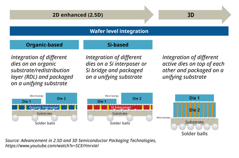
One response to the need for faster interconnections and reduced power consumption is to combine components into a single, tightly integrated unit. There are two approaches to this, known as 2.5D and 3D packaging, both offering enhanced performance, reduced size, and improved power efficiency.
As the name suggests, 3D packaging stacks dies directly on top one another, using through-silicon vias (TSVs) to connect dies vertically. This achieves higher integration density, and performance by reducing signal distances. The processing speed in today’s chips has gotten so fast that the speed of light actually becomes a limiting factor. Any reduction in signal distance results in notably better performance.
However, 3D packaging is a technically advanced and often cost-prohibitive process. 2.5D packaging serves as an intermediate step between traditional 2D packaging and full-fledged 3D packaging. In 2.5D, multiple semiconductor dies — often using different process technologies — are placed side by side on a silicon interposer that acts as a bridge, providing a high-speed communication interface. While 3D provides higher performance, size, and power consumption benefits, 2.5D still offers considerable improvements over traditional packaging.
Any thin films used in 2.5D and 3D packaging have strict functional, material, and process requirements:
- Functionally, thin films must provide the necessary high-density electrical interconnections through TSVs and redistribution layers (RDLs). Low electrical resistance and precise dimensional control are needed to ensure signal integrity and speedy data transfers. Dielectric thin films are needed to insulate the layers and minimize crosstalk. Strong adhesion and barrier properties prevent the diffusion of metals between layers while also preventing delamination. Heat dissipation is essential in integrating such dense and high-powered components. Stress control is also important to prevent the physically delicate chips from bending or cracking.
- As for material and process requirements, precise thickness control is essential, down to nanometer scale. Uniformity in thickness and quality supports consistent performance and yield. Much of the thin film deposition must also be done at low temperatures to prevent damage to the pre-fabricated components. Material compatibility is also an important consideration, as the 2.5D and 3D packages can incorporate a wide range of different materials. Long-term reliability rounds out the thin film requirements, with the ability to withstand moisture, thermal changes, and mechanical shock being essential. If the thin film fails, the whole package fails.
Thin Films for the Future
It’s entirely possible the improvements in performance and power consumption offered by 3D packaging ultimately may not be enough to keep up with the skyrocketing usage of AI and its demands for compute and electrical power. Therefore, the search is on for new technologies with the promise to supersede silicon-based processors. Quantum computing, photonic computing, and novel semiconducting materials are all being explored as possibilities.
Quantum computing, which leverages the superposition and entanglement properties seen in quantum mechanics by using quantum bits (or qubits), promises to solve a certain class of problems faster than current computers. AWS and other players are investing heavily, indicating the quantum computing market is moving beyond infancy.
Despite its promise, quantum computers are challenged with stability, error correction, and scalability. Today’s most powerful quantum computers have only just recently surpassed 1,000 qubits in size and can only maintain stable operation for one to two milliseconds.
Through silicon vias (TSVs) made of superconducting materials deposited using thin film processes are likely to play a key role in the development of quantum computing. TSVs enable 3D packaging, alleviate interconnect crowding, enable complex and highly dense qubit circuitry, and transmit the high-fidelity signaling needed for qubit coherence. Advanced thin films will provide the glue that holds quantum computing together.
Photonic computing, which uses photons instead of electrons, promises even larger gains in processing power, but real-world implementation of the technology is likely a decade or more away. Hybrid optical-electronic systems are a near-term possibility, and thin films will also play a clear role in the interfacing between the electronic and photonic components. The problem here is silicon: You can’t make a laser out of silicon. It is difficult to convert electrical energy to optical energy, and vice versa, on a single chip. Gallium arsenide and gallium nitride chips are capable of creating light, as with LEDs, but they cannot support complex logic devices. Some level of integration is required.
Novel semiconducting materials, such as graphene and wide-bandgap semiconductors, may also play a role.
Wide bandgap materials are of interest because they are capable of creating qubits that are stable, durable, and operate at room temperature or higher. The wide bandgap can help prevent the qubits from losing their quantum state to environmental noise while also enabling faster switching speeds and higher power density.
Graphene’s quantum properties, such as its high electron mobility and the ability to control its band structure, make it a promising platform for creating qubits. Other unique properties of graphene, such as its thermal conductivity and mechanical strength, also make it a strong candidate for advanced computing applications. Graphene is generally gapless, but researchers are working on creating semiconducting graphene with a bandgap by engineering it or combining it with other materials. Wide bandgap materials such as silicon carbide can be used as a substrate to grow graphene, allowing for easy integration into existing semiconductor manufacturing processes.
Conclusion
While AI applications will no doubt become more efficient in their use of compute power, it is clear the growing use of AI applications will lead to an ever-increasing demand for data centers to run the applications and also the electricity, water, and other resources needed to run them. This growth is outstripping the performance increases seen in traditional silicon-based semiconductor technology, signaling a potential end to Moore’s Law, so new technology paradigms are being explored to deliver the compute power needed for these advanced, compute-intensive applications.
As the industry shifts to 3D and 2.5D chip architectures, novel semiconductors, quantum computing, and photonic computing, thin films will play a key role.
See How Denton Can Help.
Explore how Denton’s leadership in the control of ion energy and the flexibility of its entire product line can help you create the exact thin film process you need.