Posted on
As the push for smarter, faster, and more energy-efficient optoelectronic devices intensifies, the role of innovative materials becomes increasingly important. From atomically thin graphene to multifunctional tandem structures, these advanced thin films are enabling breakthroughs in displays, photovoltaics, imaging, sensing and a host of other applications. This article explores some of the most promising materials and how Denton Vacuum deposition platforms support their development and scalable implementation.
Included in this discussion are:
- Graphene & Transition Metal Dichalcogenides (TMDs)
- Perovskite Nanowire Arrays & Heterostructures
- Metal-Selenide Heterostructures
- Amorphous Silicon (a-Si)
- Tandem Structures
Each of these materials offer their own exceptional properties, but each also requires careful handling during thin film deposition to optimize for the properties desired in the final product. Denton offers thin film solutions to meet the exacting requirements needed in using these advanced materials.
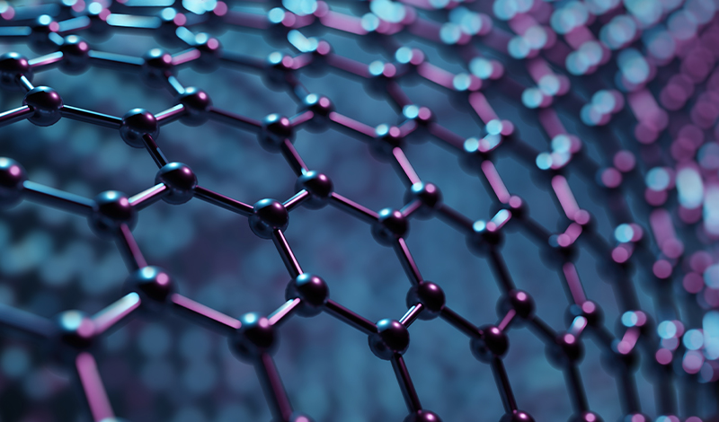
Graphene & Transition Metal Dichalcogenides (TMDs)
Graphene and transition metal dichalcogenides (TMDs) such as MoS₂ are at the forefront of next-generation optoelectronics, owing to their exceptional electrical, optical, and mechanical properties. Graphene’s unmatched conductivity and flexibility, combined with the direct bandgap exhibited by monolayer TMDs, make them indispensable for applications like photodetectors, transparent electrodes, flexible displays, and high-mobility transistors.
Traditional Deposition Methods
Traditionally, low-pressure chemical vapor deposition (LPCVD) on copper foils has been the benchmark for producing high-quality, large-area graphene. While this method yields excellent crystallinity, it requires high temperatures and involves complex transfer steps that are not ideal for flexible substrates. Alternatively, plasma-enhanced CVD (PE-CVD) enables lower-temperature growth directly on target substrates, offering a more integration-friendly route—though it demands careful optimization to control defect density and maintain film quality.
For TMDs, techniques such as atomic layer deposition (ALD), metal-organic CVD (MO-CVD), and thermal CVD provide excellent control over layer thickness and stoichiometry. However, these methods often fall short in deposition rate, area scalability, or compatibility with flexible and thermally sensitive substrates—key requirements for practical device integration.
The Denton Advantage in Graphene and TMDs
This is where Denton Vacuum’s Voyager and Phoenix PIB-CVD platforms deliver a decisive edge. These systems uniquely combine plasma-ion beam technology with CVD, enabling:
- Independent control of ion energy and flux, allowing precise tuning of film properties such as crystallinity, defect densities, and stress.
- Low-temperature processing, crucial for polymer and other temperature-sensitive substrates used in flexible electronics.
- Large-area uniformity, supporting industrial-scale manufacturing with consistent film performance.
- Monolayer precision with low defect density, critical for the performance of 2D materials in optical and electronic devices.
Unlike conventional PE-CVD or ALD systems that may sacrifice throughput for precision or vice versa, Denton’s PIB-CVD tools strike the right balance—offering scalability and wide range process tunability in a single platform. This makes them exceptionally well-suited for the deposition of 2D materials and heterostructures in flexible optoelectronics.
Perovskite Nanowire Arrays & Heterostructures
Perovskite nanowires and heterostructures have exceptional optoelectronic properties due to their unique structural and compositional features. Nanowires offer high aspect ratios, low defect densities, and enhanced charge transport, while both nanowires and heterostructures exhibit tunable bandgaps, strong light absorption, and long carrier lifetimes. Heterostructures require precise interface engineering and compositional control but enable tailored and enhanced functionalities. These properties make them highly promising for applications in solar cells, LEDs, and photodetectors, with ongoing research focused on improving stability and device performance.
Traditional Deposition Methods
Depositing perovskite nanowires and heterostructures involves various methods, each with distinct advantages and disadvantages. Solution-based techniques, like spin-coating and colloidal synthesis, offer a simple and low-cost deposition method. However, it has limited scope for large-area deposition, and lacks precise control over nanowire orientation and heterostructure interface quality. Vapor-phase methods, such as chemical vapor deposition (CVD), provide superior control over morphology and composition, yielding high-quality, crystalline structures. Yet, CVD often requires complex equipment and higher processing temperatures, limiting scalability and substrate compatibility. Furthermore, for heterostructures, controlling the interfaces between different perovskite layers is very difficult, leading to unwanted mixing of the materials. Therefore, the choice of deposition method hinges on balancing desired material quality with processing complexity and cost.
Hybrid approaches combining plasma-enhanced chemical vapor deposition (PE-CVD) and sputtering offer significant advantages for depositing perovskite nanowires and heterostructures. PE-CVD provides precise control over the chemical composition and crystallinity of the perovskite material, enabling the formation of high-quality films with tailored properties. Sputtering, on the other hand, allows for the deposition of metallic or oxide layers with excellent uniformity and adhesion, crucial for creating heterostructures or incorporating electrodes. By integrating these techniques, researchers can achieve complex architectures with optimized interfaces and controlled material properties. This combination allows for precise control over stoichiometry, film thickness, and interface quality, leading to enhanced device performance and stability compared to single-method deposition.
The Denton Advantage in Perovskite Nanowire and Heterostructure Deposition
The Denton Versa cluster platform, integrating PE-CVD and sputtering modules, offers a significant advantage for perovskite nanowire and heterostructure deposition by enabling seamless, multi-step processing within a controlled vacuum environment. This integrated approach minimizes interface contamination and oxide formation, crucial for achieving high-quality heterostructures with tailored optoelectronic properties. The Versa’s modular design offers versatility, allowing for customization and exploration of diverse combinations of deposition methods.
Metal-Selenide Heterostructures
Metal selenide heterostructures—combinations like MoSe₂/WSe₂ or ZnSe/CdSe—are attracting significant interest due to their engineered electronic, optical, and electrochemical properties. By stacking different metal selenide layers with complementary characteristics, researchers can design materials with tunable bandgaps, enhanced conductivity, and abundant active sites. These properties open the door to a wide range of applications, including photovoltaics, infrared photodetectors, thermoelectrics, supercapacitors, and even biomedical therapies such as photothermal cancer treatment.
Traditional Deposition Methods
However, to fully exploit these heterostructures, the deposition process must deliver atomic-level precision: Crystal structure, stoichiometry, and interface sharpness all directly influence device performance. This presents a challenge, particularly when scaling beyond the lab.
Traditional techniques each offer strengths but come with trade-offs:
- MBE (Molecular Beam Epitaxy) excels in interface sharpness and crystalline quality, but it is slow and costly—better suited for prototyping than production.
- CVD/MOCVD offers reasonable throughput and decent film quality but often struggles to maintain abrupt heterointerfaces.
- ALD is unmatched for conformal coatings on 3D structures and atomic-level thickness control, yet it typically produces amorphous or poorly crystalline films unless followed by high-temperature annealing.
- Sputtering/PLD enables scalable, polycrystalline film growth but often sacrifices interface purity and phase control—especially critical for complex selenides.
The Denton Advantage in Metal Selenide Heterostructures
Denton’s advanced deposition platforms—Infinity Ion Beam Deposition (IBD) and Biased Target Sputtering (BTS)—offer a distinct advantage with their exceptional precision and process control.
- IBD provides precisely tunable ion energy and directionality, enabling the growth of dense, uniform films with improved crystallinity and interface sharpness.
- BTS offers excellent control of thin film interfaces, provides independent control over ion currents and energies. This eliminates contamination and scatter from beam overspill, prevents surface damage, enables tight stress control, and creates dense, defect-free films.
Both systems operate at low pressures, reducing gas-phase scattering and contamination risk. However, a key advantage with BTS is the high film purity – ions primarily sputter the biased target, minimizing contamination from the chamber. Compared to conventional sputtering, Denton’s tools deliver higher-quality, defect-minimized films with better stoichiometric control and more repeatable results.
In essence, Denton’s IBD and BTS platforms bridge the gap between lab-scale precision and scalable manufacturing, making them ideal for companies and research labs aiming to commercialize next-generation optoelectronic and energy devices based on complex heterostructures.
Amorphous Silicon (a-Si)
Amorphous silicon (a-Si), particularly in its hydrogenated form (a-Si:H), continues to be a cornerstone in large-area electronics thanks to its low processing temperature, compatibility with a wide range of substrates, and cost-effective deposition. Despite its relatively lower carrier mobility compared to crystalline silicon, a-Si:H remains indispensable in applications that prioritize scalability and integration over speed, such as thin-film solar cells, flat-panel displays, and digital radiography systems.
Traditional Deposition Methods
The key advantage of amorphous silicon lies in its ability to be deposited uniformly over large areas at low substrate temperatures, making it compatible with flexible and temperature-sensitive substrates. Its high optical absorption in the visible range is exploited in photovoltaics, while its conformal deposition capabilities are vital for thin-film transistors (TFTs) in LCD and OLED backplanes. Additionally, in medical imaging devices such as X-ray detectors, a-Si enables the creation of large-area photosensitive arrays with adequate resolution and reliability.
The Denton Advantage in Amorphous Silicon
Denton Vacuum’s Voyager and Phoenix PIB-CVD platforms offer complementary technologies tailored to the unique challenges of a-Si deposition. The Voyager PIB-CVD system is designed for low-temperature, high-uniformity film growth across large wafers—essential for high-throughput production of TFTs and solar cells. Its advanced plasma control and multi-gas compatibility support the precise incorporation of dopants and multilayer structures, making it suitable for both intrinsic and doped a-Si:H layers. In contrast, the Phoenix PIB-CVD platform adds value through its ability to do roll-to-roll processing for large area flexible substrates. Both systems have the unique advantage for independent control of ion flux and ion energy which enables layer-by-layer growth, reducing defect density and enhancing interface quality—key for high-efficiency tandem solar cells and emerging flexible or curved electronics.
Together, these platforms provide a robust toolkit for industries aiming to scale amorphous silicon deposition without compromising on film quality or throughput. Whether the application demands low-cost large-area coverage or high-performance device integration, Denton’s systems offer a scalable and flexible solution for next-generation electronics.
Tandem Structures
Tandem heterostructures involve layering different semiconductor materials to optimize device performance. This allows for precise control of bandgaps, leading to efficient light absorption or emission at specific wavelengths. The design facilitates improved charge carrier management, reducing losses and boosting efficiency. By combining diverse materials, functionalities can be integrated within a single device, and at nanoscale, quantum effects produce unique properties. Consequently, tandem heterostructures are employed in applications like high-efficiency solar cells that capture a wider spectrum of light, advanced LEDs with tailored emissions, sensitive photo detectors, high-performance transistors, and also in research for new laser technologies, and even photocatalysis.
Traditional Deposition Methods
Key deposition tools for heterostructure fabrication include MBE, CVD, and PVD, each with distinct strengths and weaknesses. MBE offers exceptional precision and control over film thickness and composition, crucial for high-quality heterostructures, but it’s often slow and expensive. CVD provides good uniformity and scalability, making it suitable for large-scale production, but it may have limitations in achieving atomic-level precision. PVD, encompassing techniques like sputtering, is versatile for depositing various materials and offers reasonable control, but it can result in relatively less uniform films compared to MBE. Therefore, the choice of deposition method hinges on the specific requirements of the heterostructure, balancing precision, scalability, and cost.
The precision required for these multilayer stacks—especially in maintaining interface quality and minimizing defects—demands integrated deposition systems that reduce cross-contamination.
The Denton Advantage in Tandem Heterostructure Fabrication
Denton’s Versa Cluster system is very suitable for tandem heterostructure fabrication due to its modular design, allowing for the integration of multiple deposition techniques such as PE-CVD, IBD, BTS and other modules within a single ultra-high vacuum environment, minimizing contamination and ensuring precise control over film growth. This flexibility and precision, combined with potential for increased scalability and integrated processing, makes it ideal for producing high-quality heterostructures with tailored properties, crucial for advanced optoelectronic and electronic devices.
Conclusions
The evolution of next-generation optoelectronic devices hinges on the advancement and integration of novel materials—each offering distinct electrical, optical, and structural benefits. From atomically thin 2D materials like graphene and TMDs to complex architectures like tandem heterostructures and perovskite nanowires, the performance gains rely not only on material innovation but also on the ability to deposit them precisely and scalably.
Denton Vacuum’s advanced deposition platforms—including Phoenix PIB-CVD, Infinity IBD/BTS, and Versa Cluster systems—are engineered to meet these exacting requirements, offering the control, versatility, and throughput necessary for translating cutting-edge materials into high-performance devices. As the demand for faster, smaller, and more efficient technologies grows, the synergy between materials science and deposition engineering will remain at the heart of future breakthroughs.
See how Denton’s thin film deposition solutions might be used in developing and implementing the advanced materials needed for your applications. Contact us today.