Posted on
Secondary ion mass spectroscopy (SIMS) is a technique for compositional analysis of solid surfaces (such as semiconductors) in which material is removed from a surface by ion beam sputtering and the resultant positive and negative ions are analyzed in a mass spectrometer. This technique can be used to analyze the composition of semiconductor devices and thin films, or to end an etching process at the exact layer of interest. SIMS is recognized as one of the most sensitive elemental and isotopic surface analysis techniques available.
Why use SIMS?
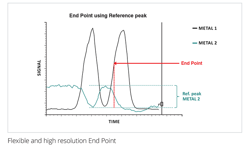
SIMS is well-suited for the semiconductor industry because of its combination of high sensitivity with good depth and lateral resolution. The areas of interest for SIMS in semiconductors include materials research, development of new processes, and process control such as etch end-pointing. For example, when etching an insulating layer deposited on a metal layer, SIMS signals when the insulator is removed and the metal layer is starting to be etched, and the etch process can be stopped.
How it Works
When an energetic ion impinges on a solid surface, atoms from the surface are ejected or “sputtered”. A fraction of these ejected atoms are ionized. These so-called “secondary ions” contain information about the elemental, isotopic, and molecular composition of the surface. The ions are mass-resolved in the SIMS module to present this information in a meaningful manner, as shown on the chart above. This technique can be applied to any type of solid material – insulators, semiconductors, metals – that can be kept under vacuum.
SIMS Applications
General Applications in the Semiconductor Industry
- The detection and quantification of trace metals on wafers.
- Ultra-shallow depth profiling. The profiling of low energy implants, the profiling of ultra-shallow gate oxides, and the detection of trace elements within the native oxide requires.
- Gathering detailed inorganic and organic information of wafer surfaces for the detection of contaminants.
- Studying the chemistry of the different organic layers for OLED displays.
- Ultra-thin film analysis to calculate the minimum and maximum thickness of the film with sub-nanometer precision.
Semiconductor Failure Analysis: SIMS is used for ending the etching process at the exact layer of interest. Semiconductor devices contain multiple layers of interest, and when looking for defects it is important to understand exactly which layer is being inspected. SIMS enables stopping at a particular layer of interest.
Ion Beam Etch: SIMS is utilized for endpoint detection. With a configuration that integrates SIMS (secondary ion mass spectroscopy) as an in-situ control, ion beam etch allows you to remove layers of one material and stop immediately at the next layer.
Denton’s SIMS Systems
The Infinity FA’s fully integrated SIMS package provides the precision required to locate small defects for further analysis. The robust SIMS package is ideal for analyzing thin film removal. It is fully computer controlled for high automation and repeatability. The SIMS enables precision endpoint control in order to improve process yield.