Posted on
What is Ion Beam Delayering?
Ion beam delayering is the removal of material one layer at a time from a substrate using ion beam etch techniques. The primary objective in the delayering process is to remove material in a manner that exposes the defect location which is buried underneath the layers.
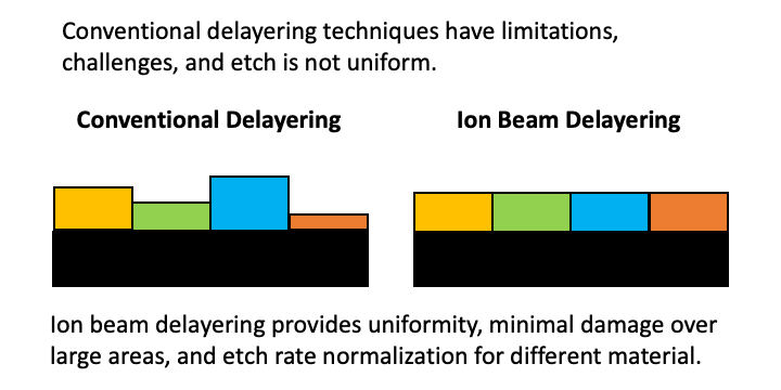
As semiconductor device nodes are getting smaller, defect identification remains a critical component of process enhancement and yield improvement. Conventional delayering methods are challenged by small feature sizes, defect isolation over large areas, surface damage to the area of interest, and high human resource overhead. Conventional delayering techniques cannot delayer devices uniformly due to different etching rates of constituent materials due to their different physical properties.
Ion beam delayering overcomes these challenges and provides uniform delayering to expose large areas of interest (AOI) while maintaining damage-free layer removal. It employs various techniques to control the accurate removal of micrometer and nanometer levels of surface material while producing a flat, planar surface. This delayering technique helps in electrical fault identification and electrical failure analysis with a large AOI and precise layer identification.
Why is Ion Beam Delayering Important?
As the microelectronics market moves to push more powerful semiconductors with higher device density, contemporary designs are shrinking the layer thicknesses and compacting the structures within the layers. Using conventional delayering techniques on contemporary chips is tedious, costly, error prone, and has limited utility.
A device must retain electrical integrity, and its surface must remain planar for failure analysis – further investigation on the root causes of the failure. In order to perform failure analysis on contemporary chips, the delayering process requires the ability to precisely remove nanometer pieces of electronic materials over the entire area of the chip.
Because of the difficulties presented by mechanical sample preparation, there has been an emergence of beam-based techniques for device delayering applications. Ion beam delayering also allows large area preparation, and a precise and controlled delayering process.
The Infinity FA System
The Infinity FA System is a high-performance etching tool designed for failure analysis sample preparation, critical thin film profiling, and delayering in semiconductor manufacturing. Ion beam etch (IBE), reactive ion beam etch (RIBE), and chemically assisted ion beam etch (CAIBE) are utilized to provide uniform etch rates for multi-material layers.
The Infinity FA System is a cost-effective, flexible solution for delayering and profiling devices with high throughput, providing rapid results and yield improvement processing at a low cost of ownership.