Posted on
Extreme ultraviolet (EUV) light requires a very complex process to produce, but this technology has major implications for lithography and nano-machining in semiconductor manufacturing. To ensure performance and precision during manufacturing, components of EUV systems must be produced with high-precision optics and coatings.
What is Extreme Ultraviolet Light?
Extreme UV light has wavelengths anywhere between 5 and 50 nm, which are about 100 times shorter than visible light wavelengths. Because of these very short wavelengths, it can be used for photolithography (etching) of fine-featured patterns. Also, because it has similar wavelengths to many atomic transitions, EUV light can be used in spectroscopic applications.
While there are sure to be more applications for EUV light in the future, right now it is used in semiconductor production, for etching patterns. It is particularly important for production of next-generation semiconductors. As feature sizes get smaller and smaller, EUV’s very short wavelengths help to meet process demands for etching patterns.
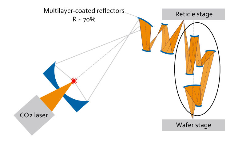
EUV Light in Manufacturing
Current EUV systems are very expensive and require very high precision. ASML, the global leader in EUV production, has developed systems that are capable of high-volume manufacturing, but the process is still very complex. A droplet generator creates tiny droplets of tin, which are then vaporized with a high-power CO2 laser in order to generate EUV light.
Ellipsoidal mirrors are used to direct the EUV light to the intermediate focus, which must be done with high conversion and collection efficiency. All of these components are at work in one very large system to create just a single EUV pulse. And because the tin droplets are so small, it’s easy to miss with the laser if precision isn’t built into every aspect of this process.
If the EUV light can be created directly from an oscillator, instead of with a generator, the laser size will decrease to a much more manageable size and cost. This technology is financially feasible for high-volume semiconductor production as feature sizes continue to shrink, and it’s already in production for those applications. But a simplified process would certainly help reduce costs for semiconductor manufacturers. It’s also a barrier when it comes to discovering new applications for EUV light and opening up R&D opportunities, which is why researchers continue to pursue other methods of producing light at these wavelengths.
Precision Optics for EUV Production
Precision optics and optical components are important pieces in EUV light systems and applications, including imaging and spectroscopy. Any optical components inside the system nearly always require a reflective surface, because EUV light radiation has extremely high absorption. Reflective coatings protect components from exposure and performance degradation over time.
Because of the extremely short wavelengths, scatter is also higher in these applications, so specs like surface roughness and surface flatness all need to be much tighter than for visible light applications. Multilayer mirrors are also commonly used in EUV systems, but they have a very narrow bandwidth, and they need to be specifically matched to the wavelength of the source beam. Precision coatings are critical to achieving this.
A thin film deposition system that’s built for precision can deliver high-performance, uniform coatings of optical components such as bandpass filters and multilayer mirrors. You’ll need to think about not just the PVD method, but the entire system configuration, to make sure you are ready to tackle EUV applications.
The biggest priority during thin film deposition is process control. Manufacturers may need to sacrifice deposition rate and invest more upfront into their system, but the ROI is worth it in order to ensure the exact right coating specs are reached. This inherently improves yield, which helps justify the greater investment.
In-situ controls like plasma emission monitoring (PEM) and optical monitoring systems (OMS) are both viable options for achieving the level of process control needed for optical components in EUV applications. PEM can actually help enhance deposition rates with real-time monitoring of the deposition process.
Find out more about how in-situ controls and ion sources can help during optical component manufacturing for EUV systems in our use case, “In-Situ Controls and Ion Sources in Action”.