Posted on
When comparing the four main types of physical vapor deposition (PVD) for thin films, it is important to know the benefits and drawbacks of each before you decide which method will best suit your application. PVD can occur through sputtering (magnetron or ion beam), which utilizes energetic ions colliding with a target to eject (or sputter) target material, or evaporation (thermal resistive and e-beam), which relies on heating a solid source material past its vaporization temperature. Previously, we compared which PVD method to use based on its benefits. In this post, we will take a deeper dive into the technical pros, cons and common uses of each type of PVD technique.
Overview of Resistive Thermal Evaporation
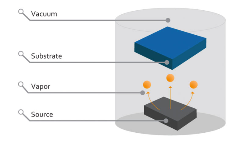
Resistive thermal evaporation applies thermal energy from a resistive heat source to a solid-state material in a vacuum chamber, which evaporates the source. The vapor condenses on a substrate, forming a thin film of the source material. It is one of the most common and simplest forms of physical vapor deposition.
Pros
- Can be used with metals or nonmetals, including aluminum, chrome, gold, indium, and is well-suited for applications using electrical contacts
- Good for materials with low melting points, such as alloys containing mercury or gallium
- Excellent uniformity if you are using planetary substrate fixturing and uniformity masks (but poor without)
- High deposition rate of <50 Angstroms per second (Å/s)
- Good directionality
- Very low cost relative to other PVD methods
- Least complex PVD process
- Compatible with ion-assist source
Cons
- Poor uniformity (without planetary and masks)
- Highest impurity levels of any PVD method
- Film quality is low density, but can be improved with ion-assist
- Moderate film stress
- Limited scalability
Uses
- Thin-film devices (OLEDs, solar cells, thin-film transistors) that require the deposition of metallic contact layers
- Wafer bonding (when indium bump deposition is needed)
- Enables the co-deposition of several components by controlling the temperature of separate crucibles
Overview of E-Beam Evaporation
E-beam evaporation, another thermal evaporation process, uses an electron beam to focus a large amount of energy onto the source material in a water-cooled copper hearth or crucible. This produces a very high temperature, which allows metals and dielectrics with high melting temperatures (such as gold and silicon dioxide) to be vaporized, and then deposited on a substrate to form a thin film. E-beam evaporation has a better deposition rate than sputtering or resistive thermal evaporation.
Pros
- Good for metals and dielectrics with high melting points
- Excellent uniformity if you are using planetary and masks (but poor without)
- Low level of impurity
- High deposition rate of <100 Å/s (better than sputtering or resistive thermal evaporation) for high throughput
- Good directionality
- High material utilization efficiency
- Compatible with ion-assist source
Cons
- Poor uniformity (without planetary and masks)
- Moderate stress resistance
- Limited scalability at reduced utilization and deposition rate
- Moderate cost and moderate system complexity
Uses
- Laser optics, solar panels, eyeglasses and architectural glass
- Good for high-volume batch production
- Metallization, lift-off, and precision optical coatings
Overview of Magnetron Sputtering
Magnetron sputtering is a plasma-based coating method where positively charged energetic ions from a magnetically confined plasma collide with a negatively charged target material, ejecting (or “sputtering”) atoms from the target that are then deposited onto a substrate. This process occurs in a closed magnetic field to trap electrons and boost efficiency—creating plasma at lower pressures which reduce gas incorporation in the film and energy losses in the sputtered atom. This method produces good film quality and the highest scalability of any PVD type.
Pros
- Good for metals and dielectrics
- Uniformity is good for better yield, although uniformity improvement can be difficult and costly
- Low level of impurity
- Film density is very good with moderate to high stress
- High deposition rate of <100 Å/s for metals, good for high throughput applications
- Highest rate of scalability (with automation available)
Cons
- Poor deposition rate for dielectrics (1-10 Å/s)
- Low directionality, but can be improved with system geometry
- High system cost and complexity
- Energetic target material can cause substrate heating
Uses
- Very dense films that require strong adhesion
- Depositing metallic or insulating coatings for specific optical and electrical properties
- Applications requiring high levels of automation
Overview of Ion Beam Sputtering
Ion beam sputtering (IBS) is a process where an an ion beam is focused on a target and sputters material onto a substrate. The process is monoenergetic and highly collimated as ions possess equal energy and directionality. This thin film deposition process results in the highest quality, densest films.
Pros
- Good for metals and dielectrics
- Excellent uniformity (the best of any PVD process)
- Very low impurity (the lowest of any PVD process)
- Produces the highest quality film of any PVD process
- Excellent directionality (highly controlled)
- Lower absorption and scatter compared to other PVD methods
- Good for low temperature applications
Cons
- Low deposition rate (1-2 Å/s)
- Low scalability, leading to lower throughput
- Slowest, most complex and expensive deposition method
- High stress
Uses
- Precision optics or semiconductor production where high-quality films are a necessity
- Ideal when durability and stability are needed
- Great when control over film thickness or stoichiometry is needed
Choosing the Right PVD Process for You
Whether deciding between thermal resistive evaporation, e-beam evaporation, magnetron sputtering or ion beam sputtering, there are a few technology criteria selections to consider. While sputtering (particularly ion beam sputtering) produces better film quality and uniformity—which can translate to higher yield— it is also more costly and complex than evaporation. On the other hand, when you’re doing high volume production and high throughput is required, evaporation offers higher deposition rates, but remember that scalability is limited. This makes evaporation ideal for large batch processing, while magnetron sputtering is better for highly automated high-volume production, particularly for thin films with short deposition times.
Any thin film PVD process decision must weigh the right balance of system cost, yield, throughput and film quality. If you need help making the right selection, contact us – we’re happy to guide you through the process.