Posted on
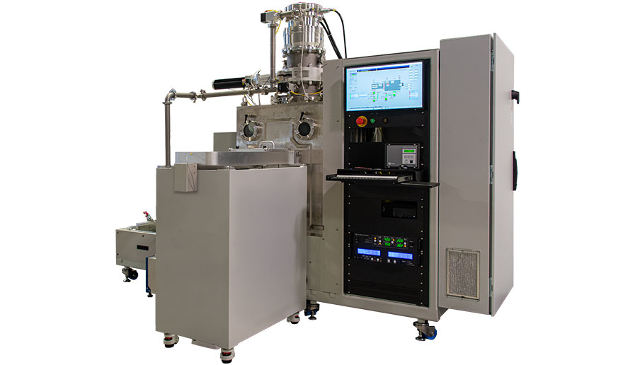
Denton strives to create product platforms that can be easily optimized to meet precise customer requirements. With that in mind, Denton has recently re-engineered the Infinity FA whole chip delayering system to be more flexible, reliable, and optimizable.
The power of whole chip delayering
The Broad ion beam etch (IBE) capabilities of the Infinity FA continue to make it a leading choice in applications requiring the delayering of an entire IC. Today’s chips are architecturally complex, often involving multiple different devices, using multiple different materials, into one advanced package.
The Infinity FA provides uniform delayering to expose large areas of interest (AOI) while maintaining damage-free layer removal. Because of its low selectivity, it can be tuned to etch uniformly through layers and features comprising multiple different materials. Its Secondary Ion Mass Spectroscopy (SIMS) module can detect the sputtering of a new layer or material in real time, stopping the etch process at the exact right point.
No other etch process can match the speed and accuracy of the Infinity FA’s Broad IBE in whole chip delayering. Focused Ion Beam (FIB) etching uses a narrow ion beam to etch and must therefore raster to perform an area etch. The time required makes it impractical to etch an entire IC. “Defocused FIB” is sometimes marketed as a broad ion beam, but its maximum beam is perhaps 2 by 2 mm, far less than the 14 cm of Infinity FA’s Kaufman-type Broad IBE.
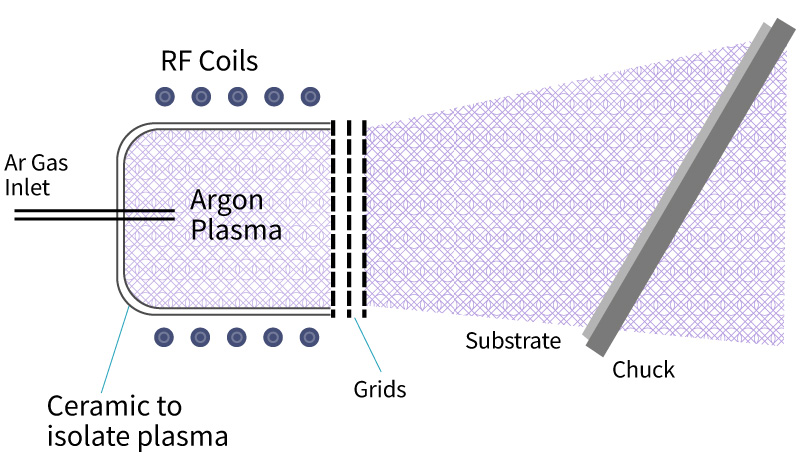
Radio frequency (RF) coils ionize the neutral argon atoms into AR⁺ and e⁻, forming a plasma. The grids accelerate the AR⁺ ions toward the substrate for etching, which the grids help optimize for uniformity.
ASM International’s International Roadmap for Failure Analysis (IRFA) Solution Gaps report [Note: paywalled content] highlights the emerging need for global IC delayering with material removal that can target a particular layer, in a timely manner, without introducing defects in the sample. The report specifically names Denton’s Infinity FA as a near-term solution, with the long-term goal of having a completely automated process for removing and analyzing materials from large areas.
For Denton, complete automation is a near-term goal. More on that in a bit.
The power of flexibility, at the right price point
Denton understands that there is no such thing as “one size fits all” when it involves thin film and etch applications. The recent tweaks to the Infinity FA create a wide variety of different options, enabling customers to find the exact right mix of capabilities at the exact right price point.
Here is rundown of the improvements:
- New form factor. Rather than use its own specialized platform, the Infinity FA is now built using the same form factor as the recently redesigned Infinity Ion Beam Etch (IBE) wafer etch system. There are several benefits to this change. It makes the Infinity FA platform easier to integrate with other Denton platforms. Using a standardized platform built around semiconductor-grade components also results in greater reliability. Finally, we can manufacture the systems more quickly, enabling Denton to deliver an optimized product to customers faster than before. Time is money, as they say.
- Easier to integrate. The Infinity FA can now be tied directly into Denton’s Versa cluster tool, enabling the creation of a fully integrated fab system with a built-in QA module, all without breaking vacuum.
- Two ion sources to choose from. Previously, the Infinity FA was only available with a Radio-Frequency Inductively Coupled Plasma (RFICP) source. While the RF ICP made the Infinity FA an incredibly powerful etch and delayering system, there are applications where this power is not needed. The availability of a Direct Current (DC) source – to be used instead of the RFICP – provides a lower-priced configuration of the Infinity FA.
Both the RFICP and DC sources deliver the Broad IBE characteristic of the Infinity FA, but the RFICP will etch 50% faster than the DC source. The RFICP is also capable of etching with oxygen, enabling chemical assisted IBE (CAIBE), which can minimize the selectivity of certain etch processes. The DC source can only etch with pure argon; it still offers superior control of selectivity, but the RFICP with CAIBE will be, by nature, more versatile. - The load lock is now optional, and more reliable. Just as not every customer needs the power of a RFICP, not every customer needs a load lock, where a large number of chips can be loaded simultaneously and then processed without breaking vacuum. The load lock is now optional, again offering a lower price point for customers who don’t need it. The load lock available on the Infinity FA is now the same as that offered on other Denton systems. This new semiconductor-grade load lock provides greater reliability.
Planning for the future
Moving to a standardized platform that is more easily integrated with other components “future proofs” the Infinity FA system for new technologies. One possible future option for the Infinity FA is tight integration with a scanning electron microscope (SEM) with digital imaging capabilities.
The IRFA Solution Gap report highlighted the importance of moving to a fully automated FA and QA capability with minimal human interaction. The incorporation of a digital imaging-capable SEM in the Infinity FA could make this a reality. A lights-out fab process incorporating an automated QA step could be implemented using Denton’s Versa cluster tool. Chips could be pulled randomly and automatically from the fab process, delayered using the Infinity FA, imaged automatically with the SEM, and evaluated. All without breaking vacuum. The evaluation of the digital SEM images could be performed using a machine learning system, or they could be evaluated remotely by a human operator. If needed, a chip could be returned to the etch process for additional etching.
Conclusion
It’s critical to use the right tool for a task. While there are a wide variety of different approaches to etching ICs for failure analysis and quality assurance – such as RIE, FIB, mechanical polishing and chemical etching – Broad Ion Beam Etching (Broad IBE) is best suited for delayering an entire semiconductor. The other approaches use a beam that is too focused, and therefore poorly suited for etching the large areas involved, or rely on mechanical or chemical means that result in damage or other artifacts.
As implemented in Denton’s Infinity FA, Broad IBE provides the necessary uniformity, minimal damage over large areas, and etch rate normalization across different materials whole chip delayering demands.
The recent tweaks to the Infinity FA platform have created a wide variety of different options, enabling customers to find the exact right mix of capabilities to suit their precise needs.
Talk to Denton today about whole chip delayering using the Infinity FA.