Posted on
The rapid expansion of Artificial Intelligence (AI) and the maturation of quantum computing are placing unprecedented demands on semiconductor manufacturing. As the limits of traditional 2D silicon scaling are reached, the industry is increasingly turning to 3D packaging and Through-Silicon Vias (TSVs) to drive performance. However, these vertical architectures introduce complex manufacturing challenges that standard deposition methods are ill-equipped to handle.
The computational requirements of Large Language Models (LLMs) and generative AI are outpacing Moore’s Law, to say nothing of the energy requirements of the data centers built to support AI applications. To meet the need for higher density and lower latency, data centers and hardware manufacturers must look to vertical integration. Stacking chips requires robust vertical interconnects, but creating these connections at the nanometer scale presents significant material science and engineering hurdles.
For hardware manufacturers, the challenge is no longer just about designing the architecture; it is about the physical reality of manufacturing it. Specifically, the difficulty lies in achieving conformal coating on the microscopic structures that enable 3D packaging. Denton Vacuum’s Plasma Ion Beam Assisted Chemical Vapor Deposition (PIB-CVD) technology addresses these challenges, offering a solution where traditional methods fall short.
The Challenge: TSVs and the “Scallop” Effect
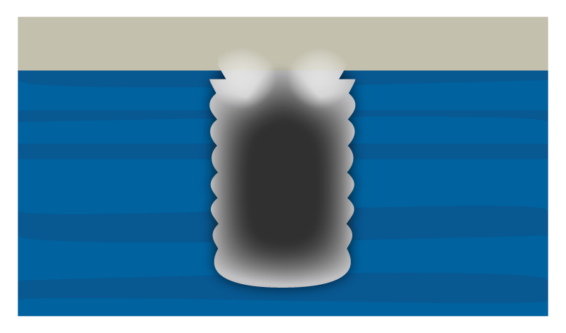
To understand the manufacturing bottleneck, one must look at the structure of the TSVs themselves. 3D packaging relies on these vias to connect stacked dies vertically, allowing for shorter signal paths and higher integration density.
Creating these deep trenches typically utilizes a Deep Reactive-Ion Etching (DRIE) technique known as the Bosch process. This method alternates between two distinct modes — an etching phase to remove silicon and a passivation phase to protect the sidewalls. By pulsing these steps, manufacturers can achieve high-aspect-ratio trenches.
However, this alternating process creates a characteristic surface roughness known as “scalloping,” resulting in microscopic ridges and undulations along the via’s sidewall. While the Bosch process is excellent for etching, it creates a difficult surface for subsequent deposition. Standard Physical Vapor Deposition (PVD) and many Chemical Vapor Deposition (CVD) processes often face line-of-sight limitations, resulting in poor step coverage on the underside of these scallops. There might be good coverage on the top of a scallop, but the area immediately beneath it remains thin or entirely bare.
In high-performance AI chips and quantum devices, discontinuous films are unacceptable. In quantum applications, where superconducting materials are often required to maintain qubit coherence, even microscopic discontinuities in the film can compromise device functionality.
The Denton Advantage: Wide Range Process Tunability
While large-scale semiconductor equipment manufacturers focus on high-volume standardization, they often lack the process flexibility required to solve these specialized problems. Denton’s PIB-CVD technology provides the necessary control to address the scalloped sidewalls of high-aspect-ratio TSVs.
Unlike standard Plasma-Enhanced CVD (PE-CVD), which often relies on substrate biasing or high temperatures to achieve film density, PIB-CVD utilizes a proprietary ion source that separates the control of ion energy from ion flux along with an ability to operate over a wide range of process pressures.
This technical distinction is critical for sidewall coverage. By independently controlling the energy and density of the ions, Denton’s systems can direct the deposition process with high precision. This allows for the creation of continuous, conformal films even on the difficult, undercut surfaces of Bosch-process scallops.
Addressing High-Aspect Ratio Requirements
The capabilities of PIB-CVD are well-proven in demanding applications. The linear source on Denton’s Phoenix platform has demonstrated the ability to deposit films on structures with high aspect ratios, with the potential to achieve a 10:1 aspect ratio.
High aspect ratios are vital for the AI market, where heterogeneous integration — packaging logic, memory, and sensors together — necessitates deeper, narrower vias.
It is equally critical for the quantum computing market. Quantum devices often utilize novel materials and require films that maintain specific electromagnetic characteristics across complex geometries. Denton’s ability to ensure conformal coverage eliminates the shadowing effects that can lead to device failure.
Flexibility for Emerging Markets
The semiconductor landscape is diversifying. While the production of standard logic and memory remains commoditized, the “More than Moore” market — comprising AI accelerators, quantum processors, and MEMS — requires specialized solutions. These emerging applications demand unique materials and the ability to coat complex, non-standard geometries.
Denton Vacuum excels in this specialized environment. By leveraging standard building blocks, Denton can create solutions tailored to these specific customer requirements.
The Phoenix platform can be configured with Denton’s patented linear ion source to support high-throughput production while delivering the specialized PIB-CVD process needed for TSVs. It offers a balance of automation and scale with the process flexibility typically associated with R&D tools.
Advanced Materials and Low-Damage Processing
A further advantage of PIB-CVD in AI and quantum applications is its low-damage profile.
Quantum bits (qubits) are notoriously fragile, highly sensitive to defects and thermal noise. Standard deposition processes that run at high temperatures (800°C to 1000°C) or require high-voltage biasing can compromise sensitive underlying structures.
PIB-CVD is inherently a low-temperature process. Because the energy for the reaction is derived from the plasma ion beam rather than thermal heat, high-quality, dense films can be deposited at temperatures below 100°C, even to room temperature. This capability allows for the coating of delicate quantum structures or polymer-based substrates without thermal degradation. Furthermore, the elimination of substrate biasing reduces the risk of electrical damage during deposition.
This flexibility extends to material selection. From diamond-like nanocomposites (DLN) for encapsulation to specialized oxides for spacers, the tunability of the ion beam allows for the transition of film properties — from polymer-like to glass-like or diamond-like — within a single chamber.
Conclusion
As the industry moves toward 3D architectures to support the next generation of AI and quantum computing, the physical integrity of interconnects becomes a defining factor in system performance.
The challenge of coating the rough, scalloped sidewalls of deep vias is significant, but solvable. With proprietary technologies like PIB-CVD, Denton Vacuum provides the precision and control necessary to enable these vertical architectures. By combining high-aspect-ratio capabilities, superior step coverage, and low-damage processing, Denton supports hardware manufacturers in building the infrastructure required for the future of computing.
If you want to learn more about Denton and our full line of thin film systems start a conversation with us.