Phoenix: Large Area Coating System for In-Line Production
Posted on
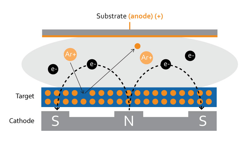
Denton’s Phoenix system platform is designed for high-volume in-line production. The system comes in two primary configurations: the Phoenix LC for magnetron sputtering with a rectangular or rotary linear cathode, and the Phoenix PIB-CVD for room-temperature chemical vapor deposition. Both systems can be configured with multiple sources to support a variety of applications. In this… Read More