Producing Graphene & TMD Thin Films for Next-Generation Optoelectronics
Posted on
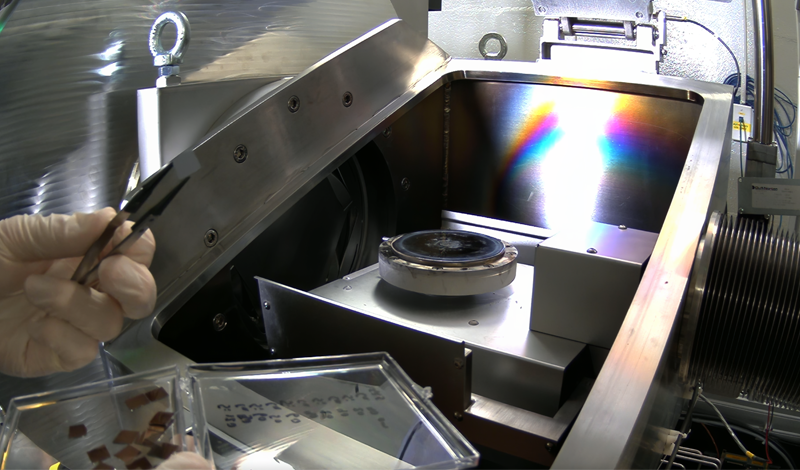
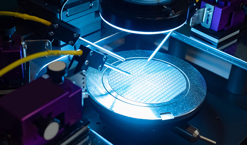
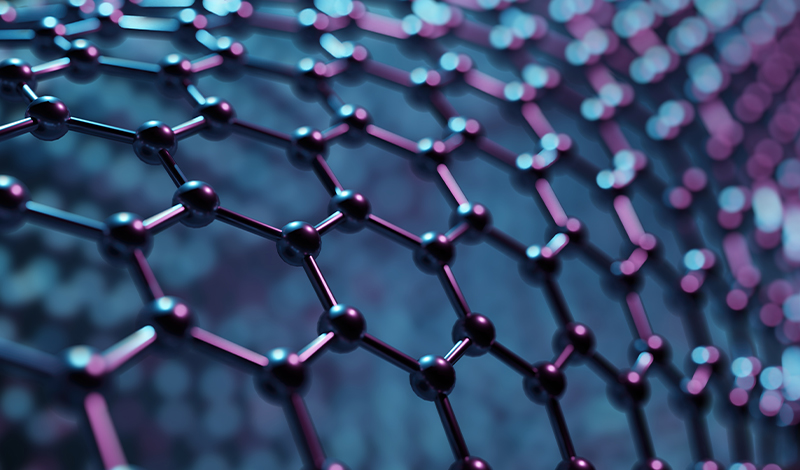
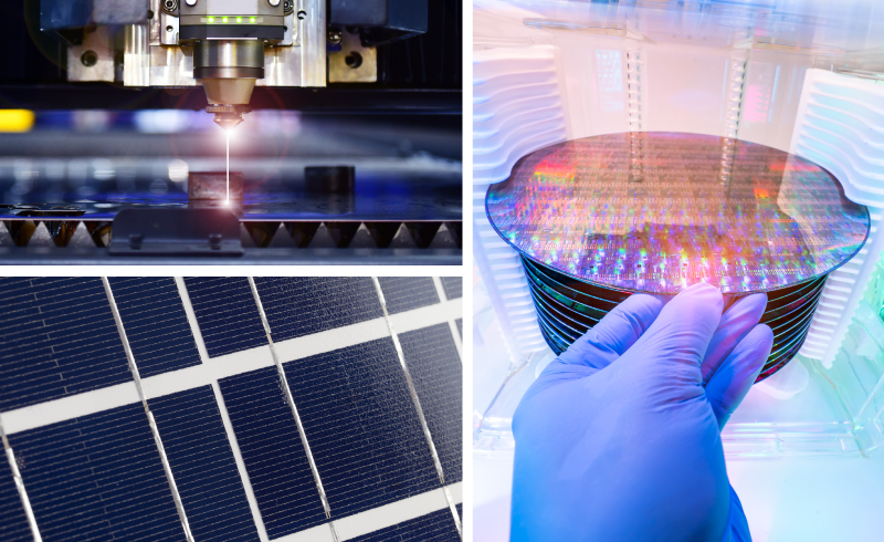
Advanced thin films – incorporating innovative materials such as atomically thin graphene – are enabling breakthroughs in displays, photovoltaics, imaging, sensing and a host of other optoelectronic devices. This video focuses on graphene and transition metal dichalcogenides, or TMDs, but Denton’s deposition platforms support development and scalable implementation of not only graphene but also: Graphene… Read More