Posted on
By adding an in-situ control or ion source to your thin film deposition system, you can achieve better performance and results, including higher yield and increased ROI. But how do you know which control choice is the right system addition for your application?
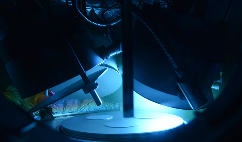
In-Situ Controls
In-situ controls allow you to observe the formation of thin film in real time, so that you can better control your deposition technique, materials and processes. With this level of real-time feedback on system performance, you’ll be able to gain tighter endpoint control over the entire deposition process. You’ll realize higher yield, repeatable results and maximum uptimes.
Two different applications for in-situ controls are plasma emissions monitoring and optical monitoring systems.
In-Situ Control: Plasma Emissions Monitoring (PEM)
Plasma emissions monitoring is a closed-loop magnetron sputtering control system that enables high deposition rates of oxide and nitride films with pure metal targets. Our solution, for example, manages reactive gas flow by monitoring plasma characteristics and adjusting the gas setpoint based on this feedback to maintain a constant rate of deposition.
PEM enables high deposition rates compared to RF sputtering and optimum film quality. If you’re looking for higher productivity in your deposition process, then a PEM application will be well-suited to your application.
Our PEM solution delivers tight integration within your thin film deposition system, giving you better process control, and is especially suited for high throughput applications.
In-Situ Control: Optical Monitoring System (OMS)
Optical monitoring systems also give you tighter process control of both sputtering and evaporation processes, by monitoring the properties of an optical thin film during deposition. Typically, this monitoring is done using the reflection of, or transmission of light through, a substrate or witness chip.
Like PEM, OMS will help you maximize yield by controlling the deposition and achieving repeatability. OMS is designed to hit on optical thickness rather than physical thickness. The result is higher production yields on precision multi-layer optics. You can use an OMS for anti-reflectance and high-reflectance, laser facets, and and filters, among other applications.
Our LamdaPro® OMS can be configured to meet your exact requirements for higher yield. It provides a high signal scan rate and analog to digital conversions, and is fully integrated into the Integrity system for easier usability. Considering an OMS? Read our older post, 2 Considerations for Accurate Optical Monitoring.
Ion Sources
Ion sources are designed to assist in the research and manufacture of optical devices, photonics and magnetic & microelectronic devices. They give you the ability to create precision films and surfaces within your system by producing and controlling ion species, and work well as an addition to ion assisted deposition and pre-clean processes.
The source produces ions with specific energy, chemical reactivity, current density and trajectory in order to effectively exercise control and create the specific film or surface you require. By controlling this ion species during deposition, you can attain desired properties such as densification, optical transmission, thickness uniformity, smooth interfaces, improved adhesion and vertical sidewalls.
Our options for ion sources are the CC-105 and our brand-new Endeavor RF ion source. The CC-105 is designed for ion assisted deposition and pre-clean processes, while the Endeavor’s filament-free design enables long runs without contamination from a filament.