Posted on
If you read our earlier publication on the scalability problems of quantum device manufacturing, you know why coating the inside of a through-silicon via (TSV) is so difficult. The etching process leaves behind scalloped sidewalls, yet most modern deposition methods are line-of-sight, making the nearly vertical surfaces an immediate challenge. Inside a quantum device, the margin for error is zero; the superconducting film must remain dense and unbroken the full depth of the via, and a single defect can be enough to compromise the device.
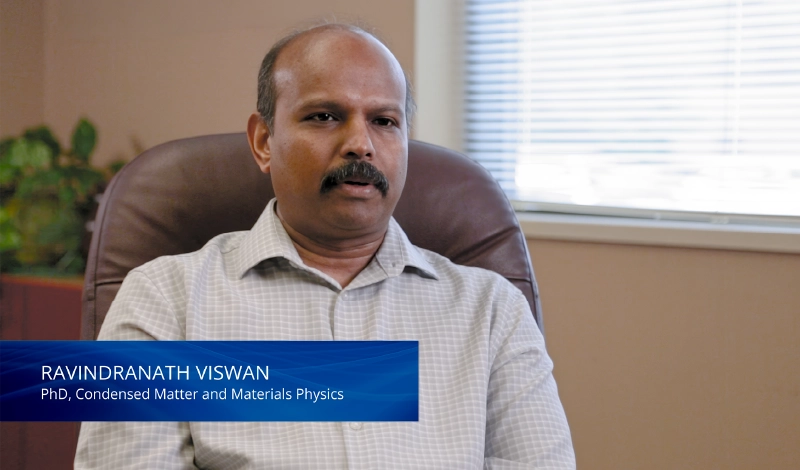
For this month’s video blog, Denton research scientist Dr. Ravindranath Viswan walks through where the research stands today. Watch below as Dr. Viswan explains:
- How Denton’s PIB-CVD and HiPIMS processes deposit dense, conformal superconducting films inside high-aspect-ratio TSVs
- What the team has coated so far
- Where the process’s real strengths lie, including the potential for major time savings
Proven at 6:1 Aspect Ratio and Ready for Next Steps
So far, the results are undeniably encouraging. Denton has coated trenches with aspect ratios of up to 6:1, producing dense, uniform films with sidewall coverage running 15 to 30% of field thickness.
Reaching that far down on a near-vertical wall is difficult enough on its own. Most deposition methods cover the top of a feature much more readily than the sides. Even when a process does reach the sidewall, holding a dense, non-porous crystalline film at a useful rate is a separate problem. By laying down highly conformal coatings while keeping the film dense, at deposition rates well beyond those of atomic-layer deposition (ALD), PIB-CVD is designed to solve both at once.
Those outcomes give us every confidence that the process can be pushed to ratios of 10:1 and likely higher. That work is underway.
Tuning the Film to the Device
Our team has already deposited titanium by HiPIMS and titanium nitride by PIB-CVD. Titanium nitride is a useful proving ground because its properties shift depending on how it’s being deposited, giving greater insight into what the process can do. PIB-CVD, meanwhile, opens up a lengthy list of independent variables to work with: ion energy, ion current density, plasma chemistry, process pressure, substrate temperature, and substrate bias. Adjusting these together shifts the film’s:
- Density
- Crystallinity
- Stress
- Composition
- Electrical behavior
- Deposition rate
In tuning them together, Denton has the opportunity to engineer a film to spec rather than settling for whatever the process produces.
Why is that flexibility so important? Simply put, quantum computing as a technology has not settled on its materials yet. New superconductors and dielectrics are still being tested, and the devices comprising the next generation of quantum hardware largely do not yet exist. In that regard, a process with this many independent controls is as much a research tool as a production one. This is ultimately why Denton sees PIB-CVD as a platform for developing materials as well as depositing them.
If you are working on advanced thin films, superconducting interconnects, or other demanding deposition challenges, our team would love to talk.
Reach out to learn about our quantum development work and discuss your deposition challenges.