See how Denton Vacuum has pioneered thin film for 6 decades.

Bias Target Sputtering for Thin Film Deposition

Laser reflecting on optic table

Posted on

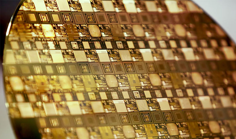
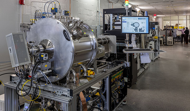
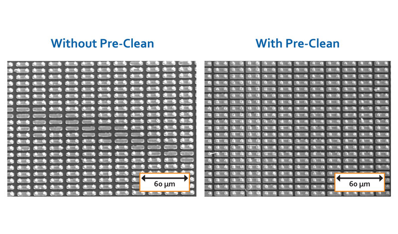
Traditional ion beam sputtering (IBS) provides excellent control over ion energies and thin film stoichiometry, making it the process of choice for sputtering metals and dielectrics for applications such as vanadium oxide microbolometers and VCSELs. Still, IBS has various challenges in meeting the necessary standards for applications in which a high degree of precision and… Read More

Cathode Options for Magnetron Sputtering

Denton Vacuum magnetron sputtering illustration

Posted on

Magnetron sputtering is a versatile deposition technique that creates very dense films with good adhesion. It can easily deposit materials with high melting points that cannot be evaporated. Denton Vacuum’s magnetron sputtering systems are highly configurable with multiple cathode options to meet the specific requirements of different applications.  In this article, we discuss the multiple… Read More

Is Evaporation or Sputtering Better for Your Application?

Robotic arm adding an OLED screen to a smart phone

Posted on

When selecting a physical vapor technique for your manufacturing process, the end application will greatly affect which technique is best. While PVD has many forms, there are two prominent techniques: evaporation and sputtering. Sputtering through magnetron or ion beam (IBS) utilizes energetic ions colliding with a target to eject (or sputter) target material. Thermal resistive… Read More

How to Prevent Defects in Thin Film Sputtering and Evaporation

Two men in sterile suits

Posted on

The goal of any thin film deposition method is to create a high-quality uniform film across the entire surface of a substrate. Unfortunately, defects such as spits, particles, and voids can interfere with your ability to reach desired film quality. If necessary, there are ways to adjust a manufacturing process to eliminate such defects and… Read More

How Can You Improve Factory Throughput in Thin Film Deposition?

Close up image of a silicon wafer

Posted on

Factory throughput in thin film deposition is one of the most critical factors affecting overall production performance. Whether you are manufacturing for high or low volume applications, you need to be able to meet production needs in the most cost-effective way possible, and scale into higher production when needed. Finding ways to raise your factory… Read More

The Customer Application Development Center at Denton Vacuum

Posted on

Welcome to the Denton Vacuum Applications Laboratory Denton Vacuum has hit a milestone with the Customer Application Development Center, the Apps Lab, as we pass the 10-year mark. The CADC empowers innovation by producing state-of-the-art sputtered, etch, and evaporated thin films and evaluating machine performances with our cutting-edge tools. In the CADC, Denton has three… Read More

Plasma Ion Beam Chemical Vapor Deposition (PIB-CVD): A New Class of Thin Film Deposition

Interview with Ravindranath Viswan

Posted on

PIB-CVD is a groundbreaking thin film deposition technology with a wide range of tunability, scalability, and durability. A primary feature of PIB-CVD is that the ion current density and the ion energy can both be independently controlled without the need for substrate biasing or additional grids. To learn more about the configurations, treatments, and other… Read More

Pre-Cleaning in Thin Film Deposition

Woman in scrubs cleaning a thin film

Posted on

The global physical vapor deposition market is expected to expand at a compound annual growth rate (CAGR) of 7.5% from 2022 to 2030. The increasing demand for this process is due to the technological advancements in the industry. PVD films are used in applications for solar cells, optical & electrical components, automobiles, wear coatings, energy… Read More

Managing Spit Defects During Evaporation

A side-by-side comparison of spit during evaporation with a standard source design, and with Denton's proprietary source design. With Denton's design, you see significantly less spit particles.

Posted on

Spit defects are some of the biggest obstacles to ensuring thickness uniformity and production efficiency in evaporation and indium bump deposition. There are ways to adjust your process to eliminate spit defects and improve yield, but if you work with a partner who has solved for these defects in their system design, you will realize… Read More

Improving Adhesion During Lift-Off For Indium Bump Deposition

Side-by-side comparison of indium bump arrays without pre-clean and with pre-clean, respectively.

Posted on

To form indium bumps, a patterned mask is applied to the wafer and then indium is deposited. The patterned mask has “holes” that allow some indium to deposit directly onto the wafer, while the rest of the indium is deposited onto the mask. After indium bump deposition, the unwanted indium and the mask must be… Read More