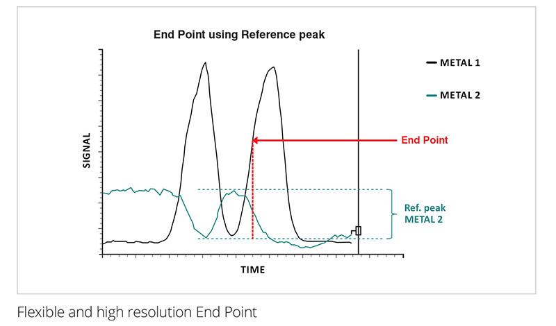
See how Denton Vacuum has pioneered thin film for 6 decades.

Utilizing Plasma in Chemical Vapor Deposition: Plasma Enhanced CVD vs PIB-CVD

Plasma Ion Beam Chemical Vapor Deposition

Posted on

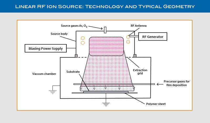
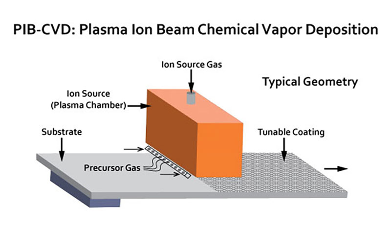
In thin films obtained by Chemical Vapor Deposition (CVD), chemical reactions are driven by applying heat to the substrate to be coated or to the area immediately around the substrate. Reactive precursor gasses are then introduced into the deposition chamber and react immediately with the heated substrate surface or combine to form new compounds that… Read More

How Can You Improve Factory Throughput in Thin Film Deposition?

Close up image of a silicon wafer

Posted on

Factory throughput in thin film deposition is one of the most critical factors affecting overall production performance. Whether you are manufacturing for high or low volume applications, you need to be able to meet production needs in the most cost-effective way possible, and scale into higher production when needed. Finding ways to raise your factory… Read More

4 Industry Applications for PIB-CVD

Posted on

In the world of thin film deposition, there are few techniques that have the versatility of PIB-CVD. Short for plasma ion beam assisted chemical vapor deposition, PIB-CVD is a cutting-edge thin film deposition process that can be used to deposit large area multifunctional thin films with greater efficiency as well as engineer new materials.  What… Read More

The Customer Application Development Center at Denton Vacuum

Posted on

Welcome to the Denton Vacuum Applications Laboratory Denton Vacuum has hit a milestone with the Customer Application Development Center, the Apps Lab, as we pass the 10-year mark. The CADC empowers innovation by producing state-of-the-art sputtered, etch, and evaporated thin films and evaluating machine performances with our cutting-edge tools. In the CADC, Denton has three… Read More

Denton Vacuum Infinity FA Tool

Posted on

Enable uniform removal of the entire layer regardless of chemical composition The Infinity FA from Denton Vacuum is optimized for delayering applications. The Infinity FA can utilize multiple etch technologies for uniform removal of layers. This high-performance etch tool is designed for delayering finished or in-process integrated circuits for failure analysis or reverse engineering. Learn… Read More

SIMS Analytics for Semiconductors

Posted on

Secondary ion mass spectroscopy (SIMS) is a technique for compositional analysis of solid surfaces (such as semiconductors) in which material is removed from a surface by ion beam sputtering and the resultant positive and negative ions are analyzed in a mass spectrometer. This technique can be used to analyze the composition of semiconductor devices and… Read More

A Look Ahead at the Semiconductor Industry

2 robotic arms manufacturing a semiconductor

Posted on

Semicon West 2022 connected business and technology leaders, researchers, and industry analysts from across the microelectronics supply chain in California and online for their annual event. Here are some key takeaways from the conference. Semiconductor Market on Track to a Trillion The semiconductor industry faced several recent challenges and has seen disruptions. A crisis response… Read More

Isoflux: The Optimal Choice for Ultrahigh Uniformity Flat Substrates

Diagram showing a cylindrical cathode configuration with the substrate inside the cathode, sputtering inward.

Posted on

Inverted cylindrical magnetron (ICM) sputtering is the optimal choice for applications that require ultra-uniform coatings on flat substrates. For example, ICM sputtering offers uniformity below 1% on standard 200mm wafers. ICM sputtering follows the same steps as conventional magnetron sputtering except a cylindrical cathode is used instead of a planar cathode. Instead of sputtering up… Read More

The Basics of Ion Beam Delayering

Posted on

What is Ion Beam Delayering? Ion beam delayering is the removal of material one layer at a time from a substrate using ion beam etch techniques. The primary objective in the delayering process is to remove material in a manner that exposes the defect location which is buried underneath the layers. As semiconductor device nodes… Read More

How to Handle Varying Wafer Sizes in Compound Semiconductor Manufacturing

A central wafer handler, with a wafer carrier, holds a semiconductor wafer and moves it between deposition chambers.

Posted on

In large-scale, high-volume silicon semiconductor production, such as for microprocessors and DRAM, manufacturers often prefer direct handling of wafers during the thin film deposition process. This makes perfect sense for mass-producing wafers that are all 300mm in size. However, in the compound semiconductor industry, multiple wafer sizes are quite common. It is not economically viable… Read More